I turn specs into things you can hold.

Chips in production cars. Firmware on real silicon. A print-ready toy from my daughter’s drawing. I work across the whole hardware chain — and run an AI engineering team that turns ideas into real hardware.

From experience to an AI engineering workflow.

I’ve designed chip architectures, analog circuits, digital logic and the systems around them. That breadth lets me connect the right knowledge, tools and engineering checks—so AI can do useful work across UltraSense.

  1. Draw

    Your spec, sketch or brief becomes precise instructions and acceptance checks.

  2. Build

    Specialist agents develop electronics, mechanics, FPGA and firmware in parallel, on shared product knowledge.

  3. Real

    Hardware, code and test records — plus a product digital twin your own team and agents can query.

I’ve worked across the entire hardware chain.

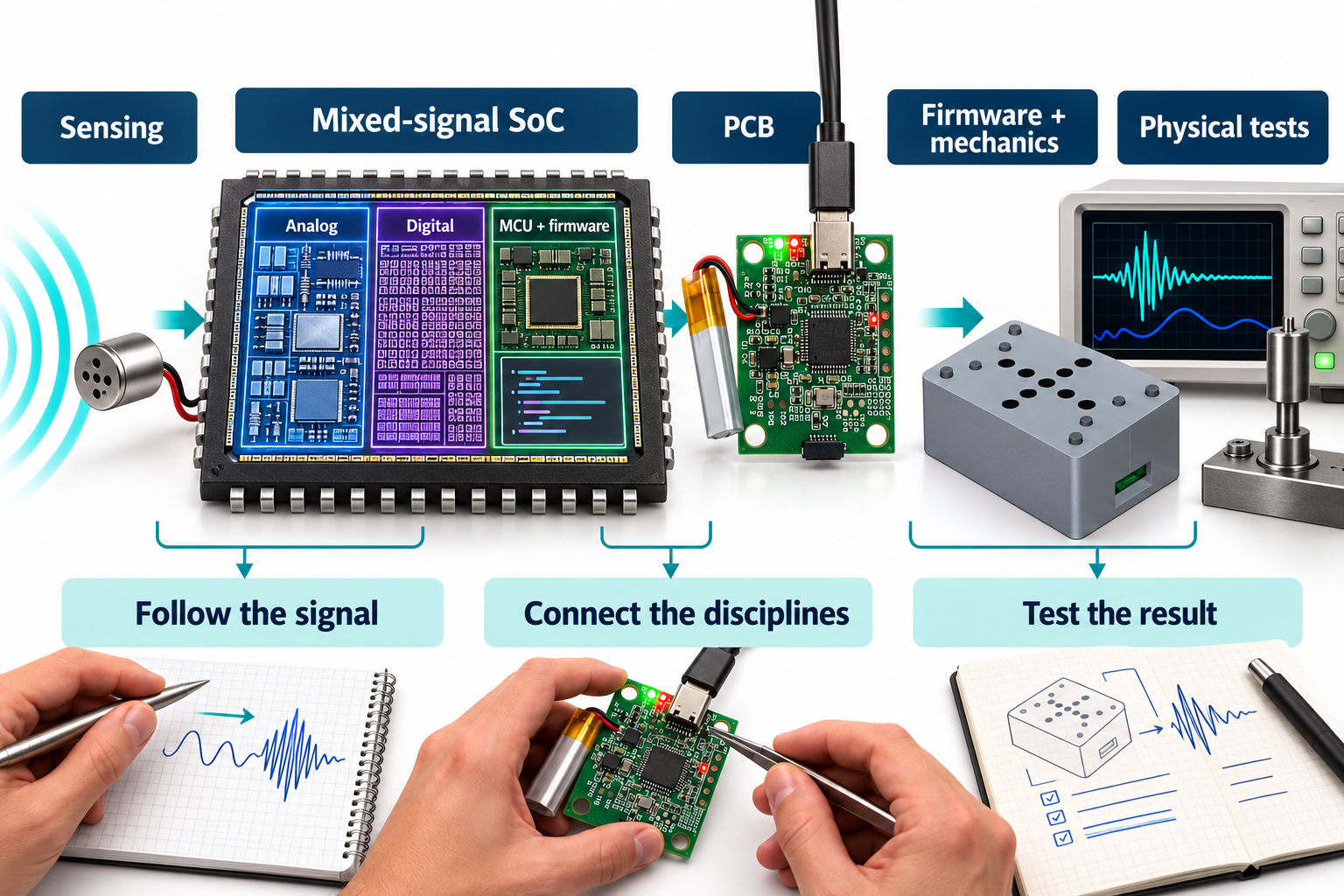
Sensors, analog circuits, digital logic and firmware running inside the chip—then the board, mechanics and experiments around it. I understand the work on both sides of each interface.

Mixed-signal SoC with analog, digital and embedded MCU firmware domains connects sensing, PCB, mechanics and physical tests.
Sensing through system verification: analog, digital and embedded-firmware domains.

At Berkeley, I developed ultrasonic transducers, interface circuits and imaging systems. At TDK-InvenSense and UltraSense, I worked across ASICs, electronics, firmware and mechanical integration.

I design what happens inside the chip.

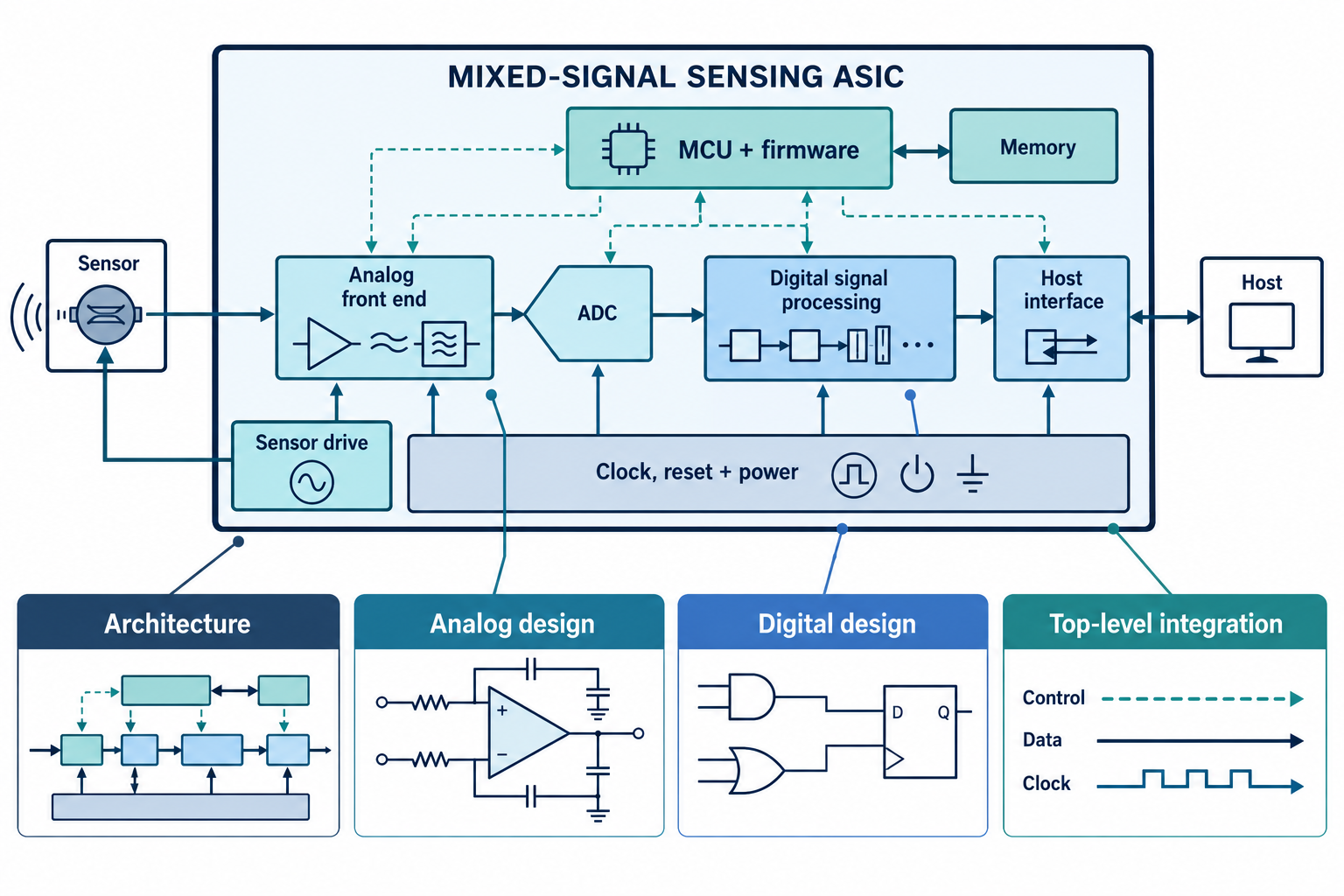
Architecture, analog circuits, digital logic, on-chip MCU + firmware and top-level integration. I understand the design decisions inside each block—and the interfaces between them.

Mixed-signal ASIC block diagram: sensing front end, ADC, digital signal processing, embedded MCU and firmware, memory, host interface, clocks and power; architecture, analog, digital and top-level integration roles.
Chip architecture, analog design, digital design and top-level integration.
Chip architecture
Partition the system and define how the blocks work together.
Analog design
Design sensing interfaces, readout circuits and signal conversion.
Digital design
Connect RTL, signal processing, control logic and embedded firmware.
Top-level integration
Bring signals, clocks, reset, memory and firmware into one working system.

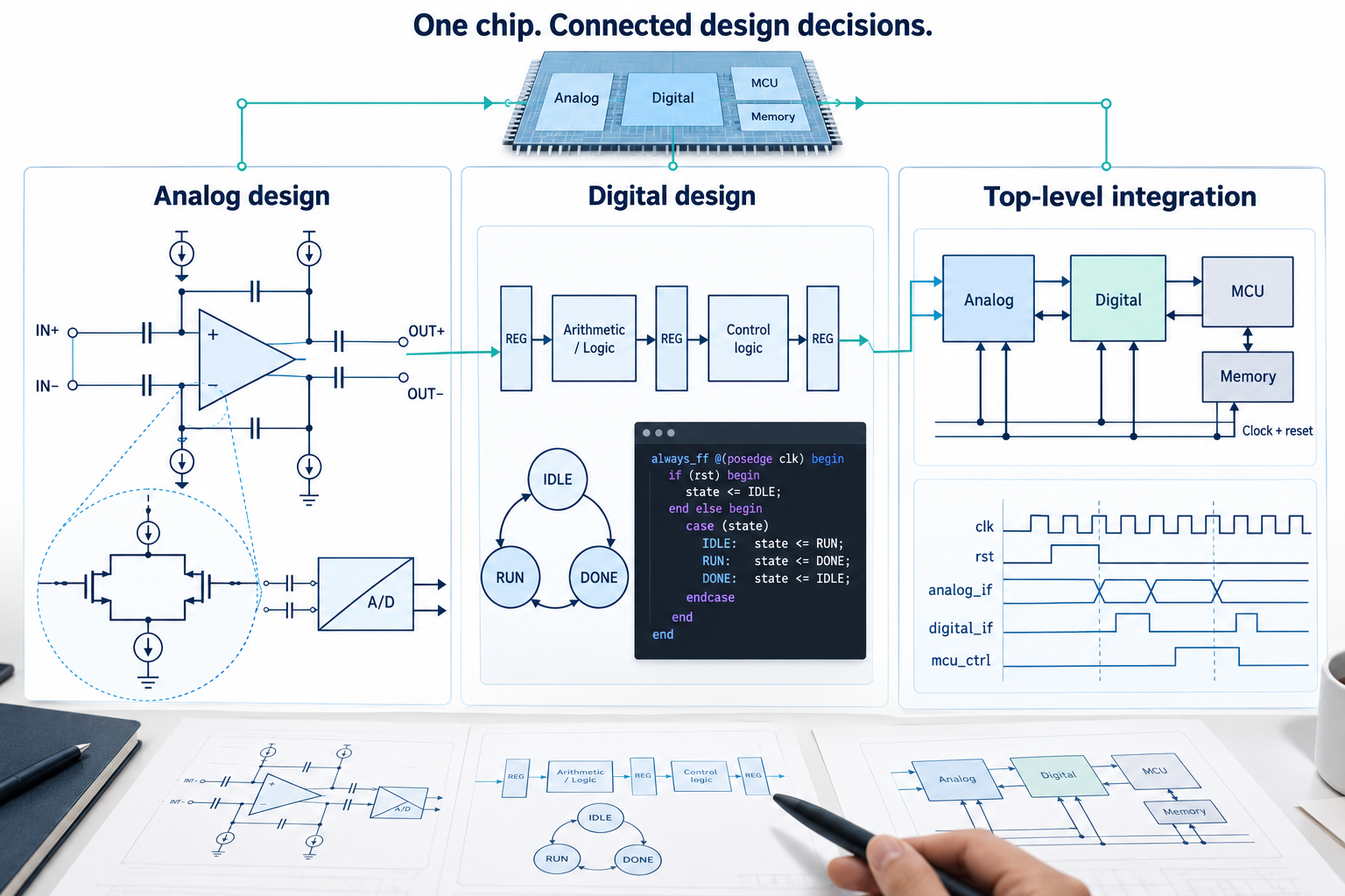
Circuit detail. Digital logic. System integration.

I can follow a design from the analog signal path through RTL and firmware to the full-chip interfaces.

Explore my circuits and chip portfolio
Analog circuit, digital RTL and state logic, and chip-level clock/reset/interface integration design views.
Analog, digital and integration design views.

Things I've made real.

D0 = the day the first chip arrived.

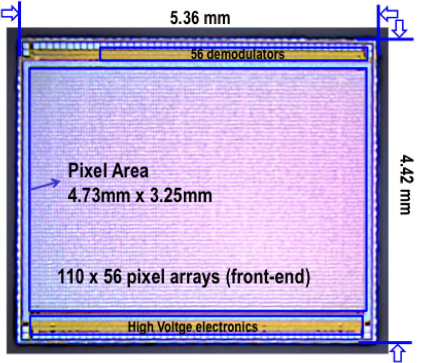
Original fabricated Berkeley CMOS fingerprint ASIC die before MEMS bonding; JSSC 2016 Figure 21.

Fabricated ASIC

My research · UC Berkeley

Research & original figure
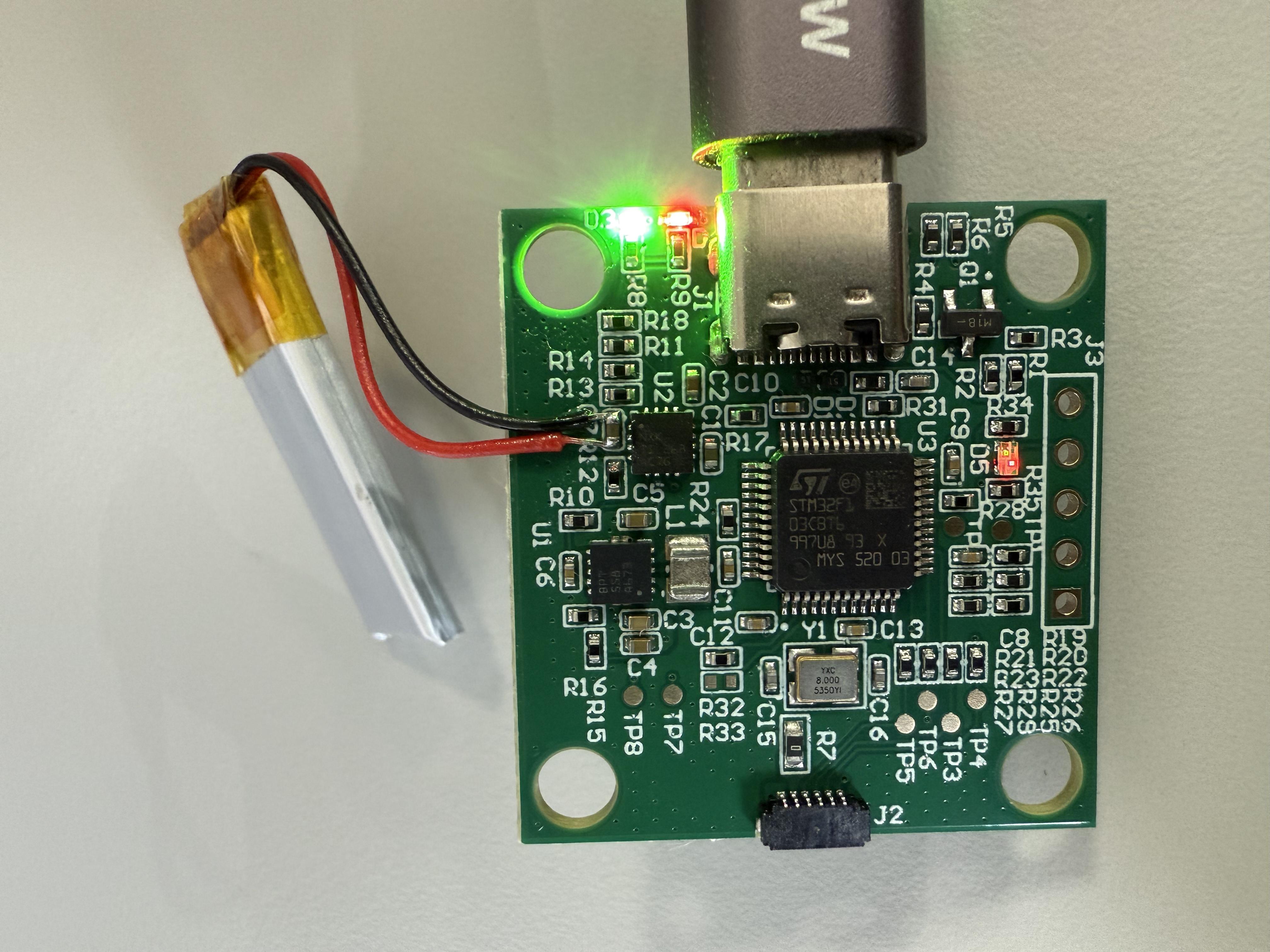
Original photograph of an UltraSense controller PCB connected to a battery and USB-C cable, with LEDs illuminated.

Controller electronics

Prior team work · UltraSense

Hardware portfolio
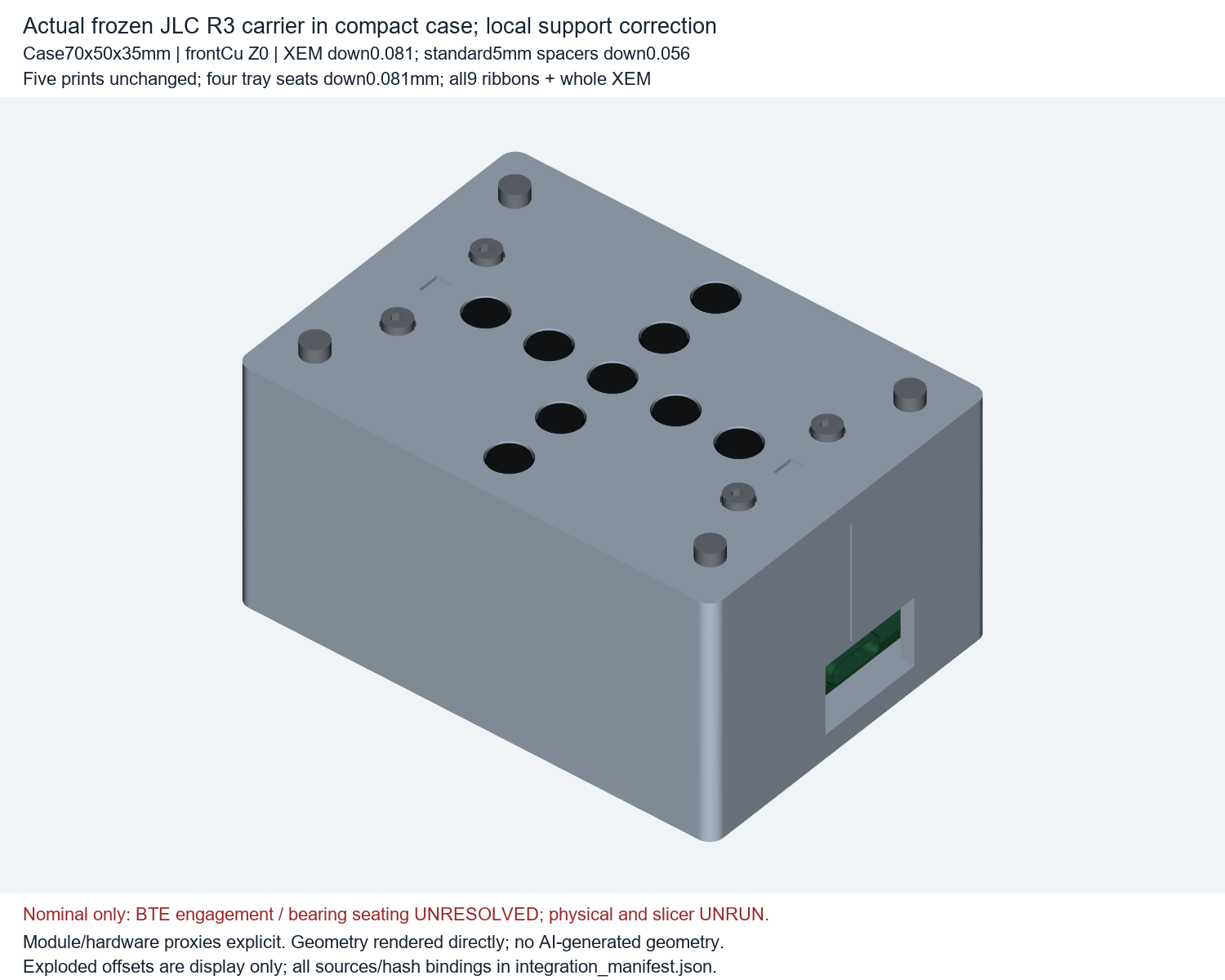
Nine-sensor array enclosure CAD with nine acoustic openings.

Mechanical CAD

Ponchi AI · EchoMind design

Design files & context
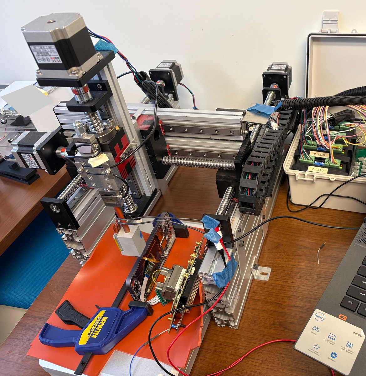
A multi-axis test platform with a sensor fixture, cables and control electronics.

Physical testing

AI workflow · UltraSense, first bring-up weeks

Experiments & results

From the circuit to the physical experiment.

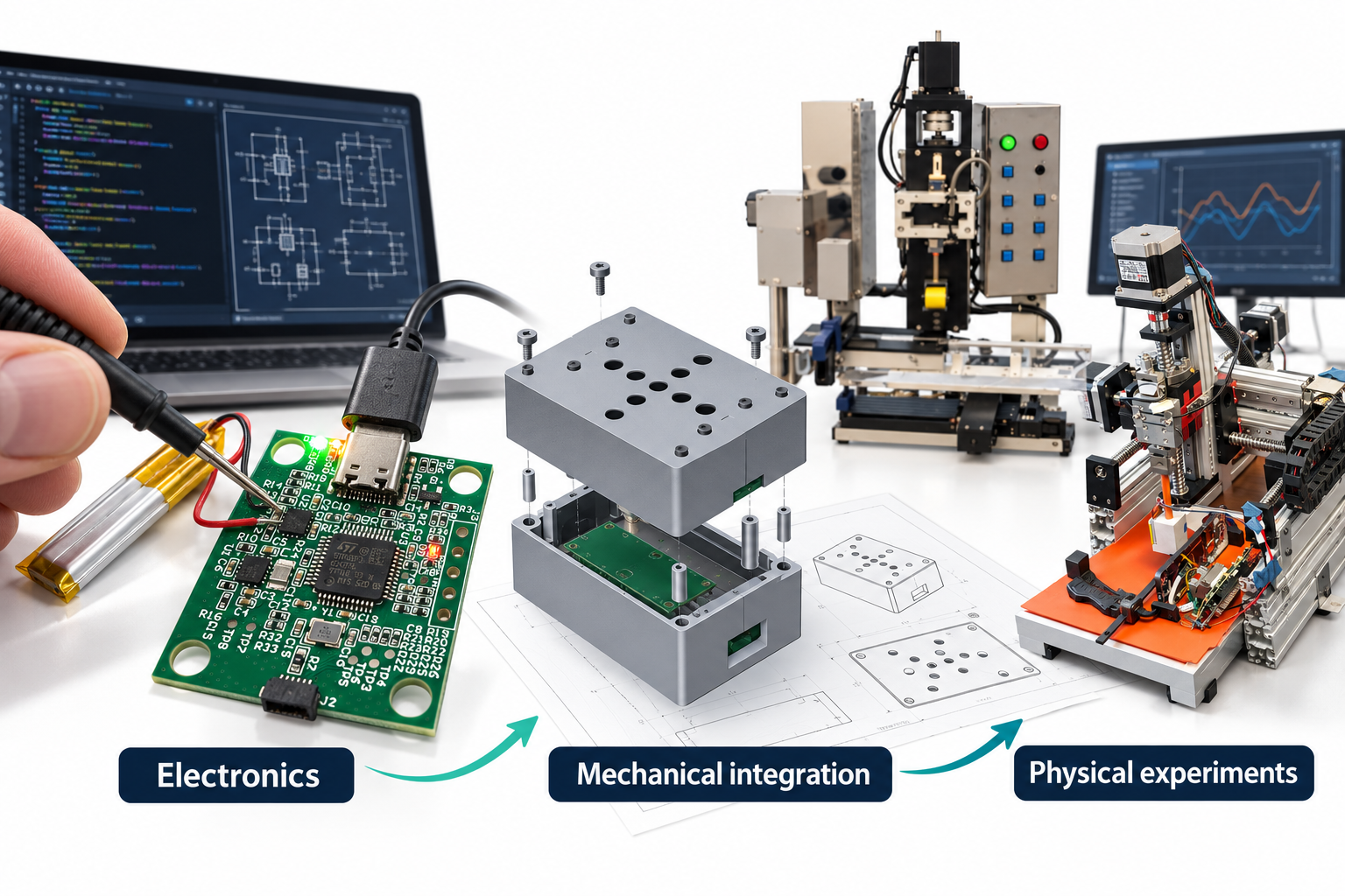
I bring electronics, firmware and mechanical constraints into the same engineering conversation. Today, I use that experience to direct AI development across PCB design, enclosure CAD and bench testing.

Portfolio composition based on original controller electronics, EchoMind enclosure CAD and two independent UltraSense physical test platforms.
Controller electronics, EchoMind enclosure CAD and UltraSense test equipment.
View the original figures
Original fabricated Berkeley CMOS fingerprint ASIC die before MEMS bonding; JSSC 2016 Figure 21.
Fabricated Berkeley CMOS fingerprint ASIC before MEMS bonding · JSSC 2016, Fig. 21.
Original photograph of an UltraSense controller PCB connected to a battery and USB-C cable, with LEDs illuminated.
Original controller-electronics photograph · prior UltraSense team work.
Nine-sensor array enclosure CAD with nine acoustic openings.
Original source-derived EchoMind nine-sensor array enclosure CAD · design view.
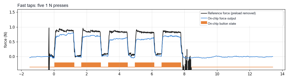
Selected measurement of five one-newton taps with reference force, chip output and button state.
Original on-chip force-sensing measurement · five 1 N fast taps, D+21.

That breadth is why my AI team builds real hardware, not slideware.

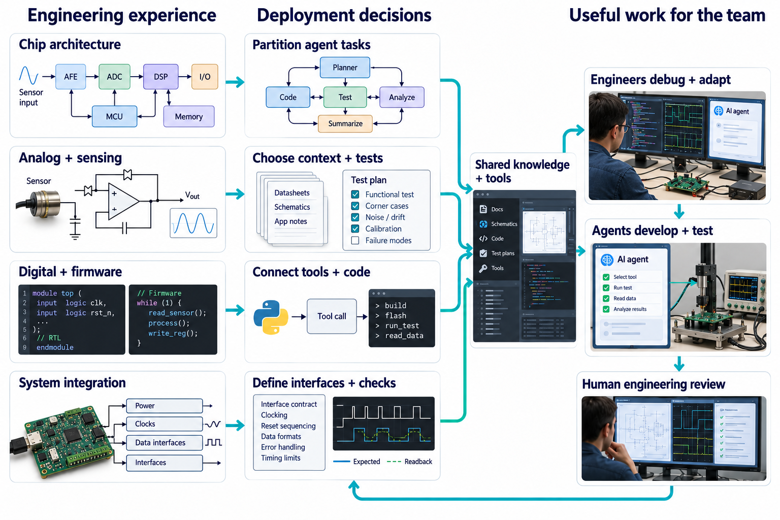
Because I’ve worked inside the chip and across the bench, I know how to turn an engineering goal into the right context, tool connections, agent tasks and acceptance checks. That is the foundation of the AI environment I deployed at UltraSense.

Causal map: chip architecture informs agent task partitioning; analog and sensing inform context and tests; digital and firmware inform tool connections; system integration informs interface and acceptance checks.
Engineering experience informs deployment decisions, shared tools and the work engineers and agents carry out.
Chip architecture
Partition agent tasks
Analog + sensing
Choose context + tests
Digital + firmware
Connect tools + code
System integration
Define interfaces + checks

Sensor simulation & design connects my PMUT and piezo transducer work with a parallel agent for multiphysics studies and hand-calculation checks.

I deployed AI across UltraSense.

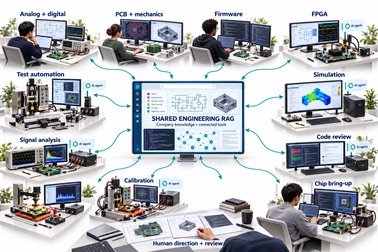
At UltraSense, I built the shared knowledge base, agent workflows and tool connections that put AI into everyday engineering. Engineers and specialist agents work across design, firmware, chip bring-up, calibration and physical tests—with common context and results the team can inspect.

Shared company engineering RAG connects engineers and specialist AI agents across chip design, firmware, PCB, FPGA, simulation, review and physical testing.
Engineers use company knowledge and connected tools; specialist agents advance development and independent test loops.
  1. Build the company’s shared context

    I connect chip knowledge, design records and test methods so engineers and agents can work from the same sources.

  2. Connect AI to engineering tools

    I build the paths from a question to code changes, debugging, firmware programming and equipment-driven experiments.

  3. Put the capability in the team’s hands

    Colleagues use and adapt the environment for their own work. I direct parallel development and review the engineering results.

Bring-up / an analog designer at the bench.

On D0, an analog designer used Claude and the prepared tools to investigate I²C communication, submit a firmware change and program the device.

View the original record
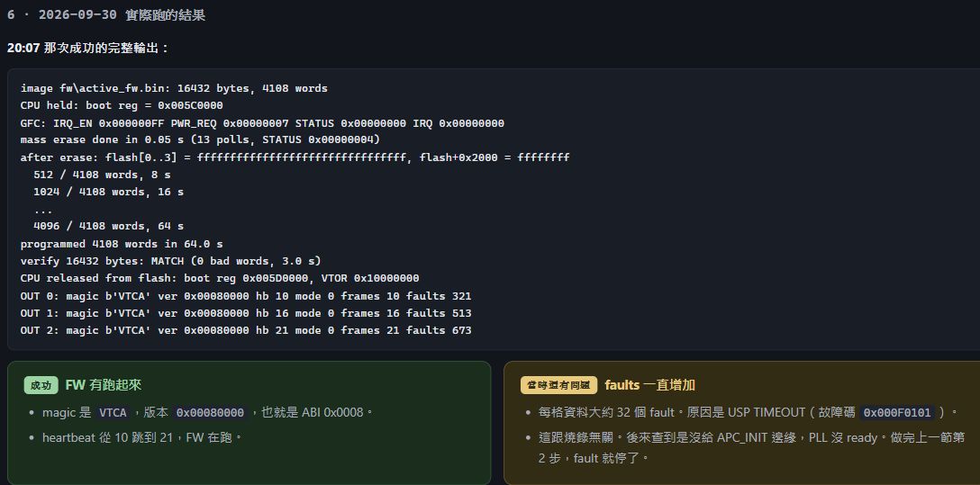
Arrival-day firmware readback and advancing heartbeat.
Day one: firmware programmed and running.

Adaptation / a workflow someone else can change.

Another engineer used his own Claude environment to make small firmware and GUI changes for tactile testing, then kept the setup for future work.

Read the adaptation record

“Introducing AI lowered the difficulty of these workflows enough for us to contribute.”

Analog IC designer · D+6 · translated from Chinese
Explore the cases, scenes and original feedback

More setups. More engineering questions moving forward.

I set the questions and review the tradeoffs. AI develops candidates and runs supported test loops across independent setups.
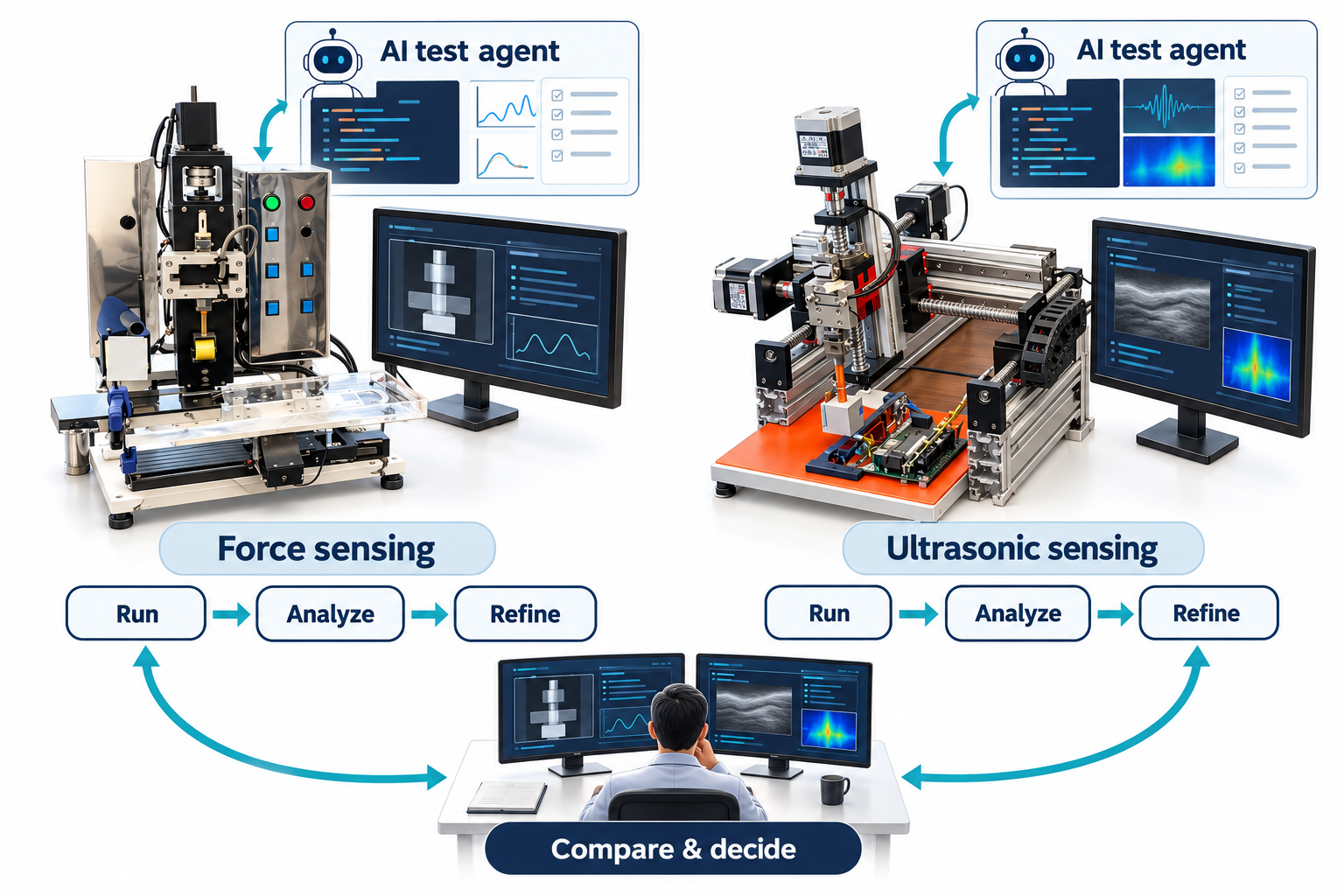
Two test platforms, each with an AI test agent and a Run, Analyze, Refine loop, returning results to human review.
Two independent test loops, from setup to analysis and the next experiment.

Force sensing

Develop firmware and press-detection candidates, run supported press tests and compare the measured response.

Ultrasonic sensing

Compare filtering and signal-analysis candidates, then carry selected changes into firmware and measurement.

Results return to me for comparison and the next decision. Agents develop and test on independent hardware loops.
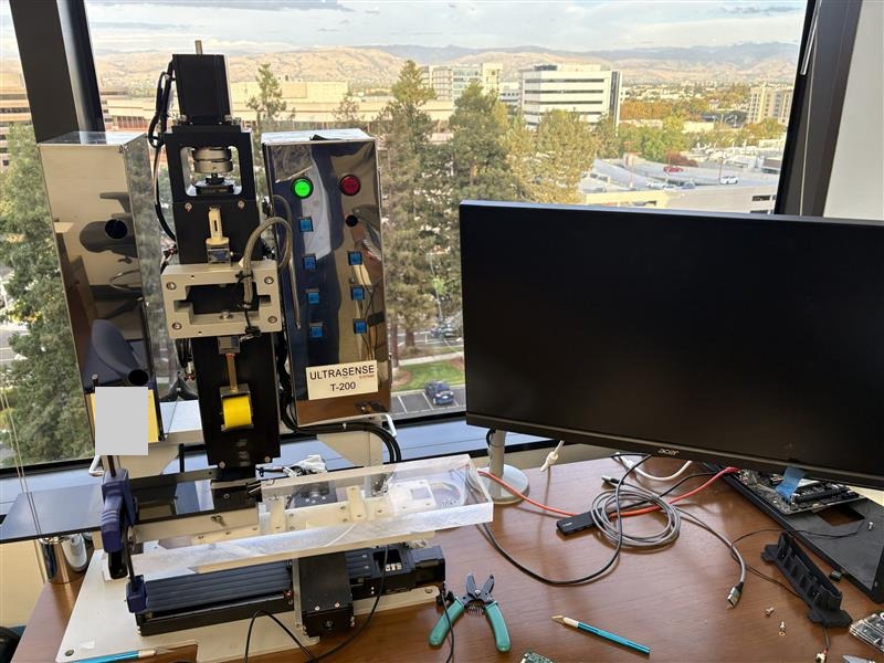
An automated press platform beside a monitor in the laboratory.
Original automated press platform and work area · UltraSense.
A multi-axis test platform with a sensor fixture, cables and control electronics.
Original multi-axis platform, sensor fixture and control electronics · UltraSense.
Read the full parallel-development case