Hao-Yen Tang

Co-founder & CTO, UltraSense

I build systems that letAI work at the bench.

Separate setups can advance separate engineering questions in parallel.

At UltraSense, I built and integrated an AI engineering environment that connects company knowledge, development tools and hardware experiments. That foundation now supports algorithm development across multiple physical setups.

See parallel development in practiceThe judgment behind it

My work spans sensing, chips, firmware and physical testing. I set the engineering direction and make the tradeoffs; AI agents implement, measure and compare the next options.

Berkeley PhD · First-author ISSCC paper awarded the Lewis Winner Award

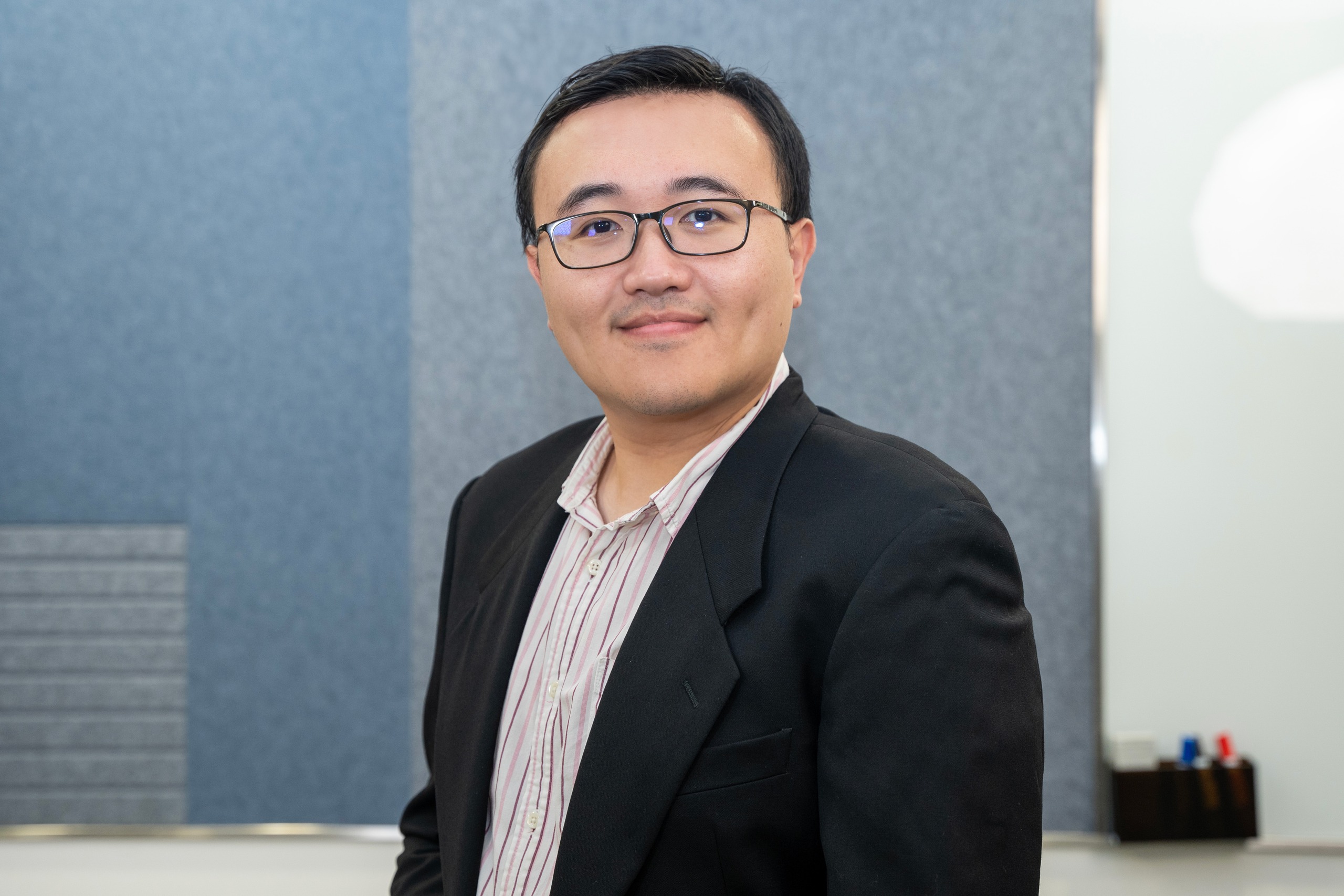
Hao-Yen Tang in his office
Hao-Yen Tang / Hardware × AI

THE LATEST CHAPTER

From shared tools to parallel experiments.

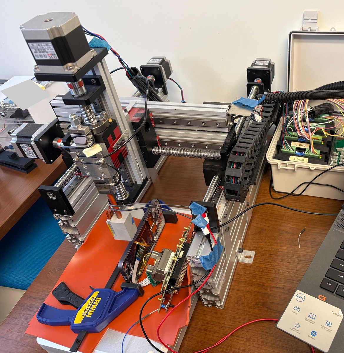
Once the knowledge and tools were connected, I could carry an engineering question into more than one setup. One track worked on force sensing with an automated press rig. Another worked on ultrasonic measurements, filtering and firmware.

I choose the questions, prepare the physical setup and decide which tradeoffs matter. AI agents develop candidates, run supported tests and compare results. That keeps several lines of investigation moving, with each experiment shaping the next round.

See parallel development in practice
A multi-axis test platform with a sensor fixture, cables and control electronics.
A multi-axis test platform, sensor fixture and control electronics.
Shared knowledge. Independent physical setups.Engineering goals · company knowledge · code and test methods

Setup A / Force sensing

Stable force output and reliable press detection

  1. DevelopCandidate algorithms and firmware
  2. MeasureAutomated press rig and reference force
  3. ComparePress detection, drift and false triggers

Firmware iteration and repeatable press campaigns

Results guide the next candidate

Setup B / Ultrasonic sensing

Better signal quality within a processing budget

  1. DevelopFiltering, calibration and firmware
  2. MeasureSeparate sensing board and capture interface
  3. CompareRecorded signal quality and processing cost

Filter research followed by firmware integration

Results guide the next candidate

Concept workflow based on the two development tracks. Engineers set objectives, prepare hardware and choose tradeoffs.

Each physical setup is an independent development resource. Sessions sharing one rig take turns controlling it.

Keep experiments running beyond the workday.

Automated campaigns continue through configured test conditions between engineering decisions, so the next workday starts with fresh measurements and comparisons.

Where engineering judgment matters

Define improvement

Prioritize stable force output and normal press detection, then evaluate slow presses and long holds against those goals.

Check the measurement

Use the measured reference force to distinguish a light-press delivery problem from an algorithm problem.

Match checks to the change

Check candidates in software, test them on the chip and keep a path back to the previous firmware.

A change the team could feel.

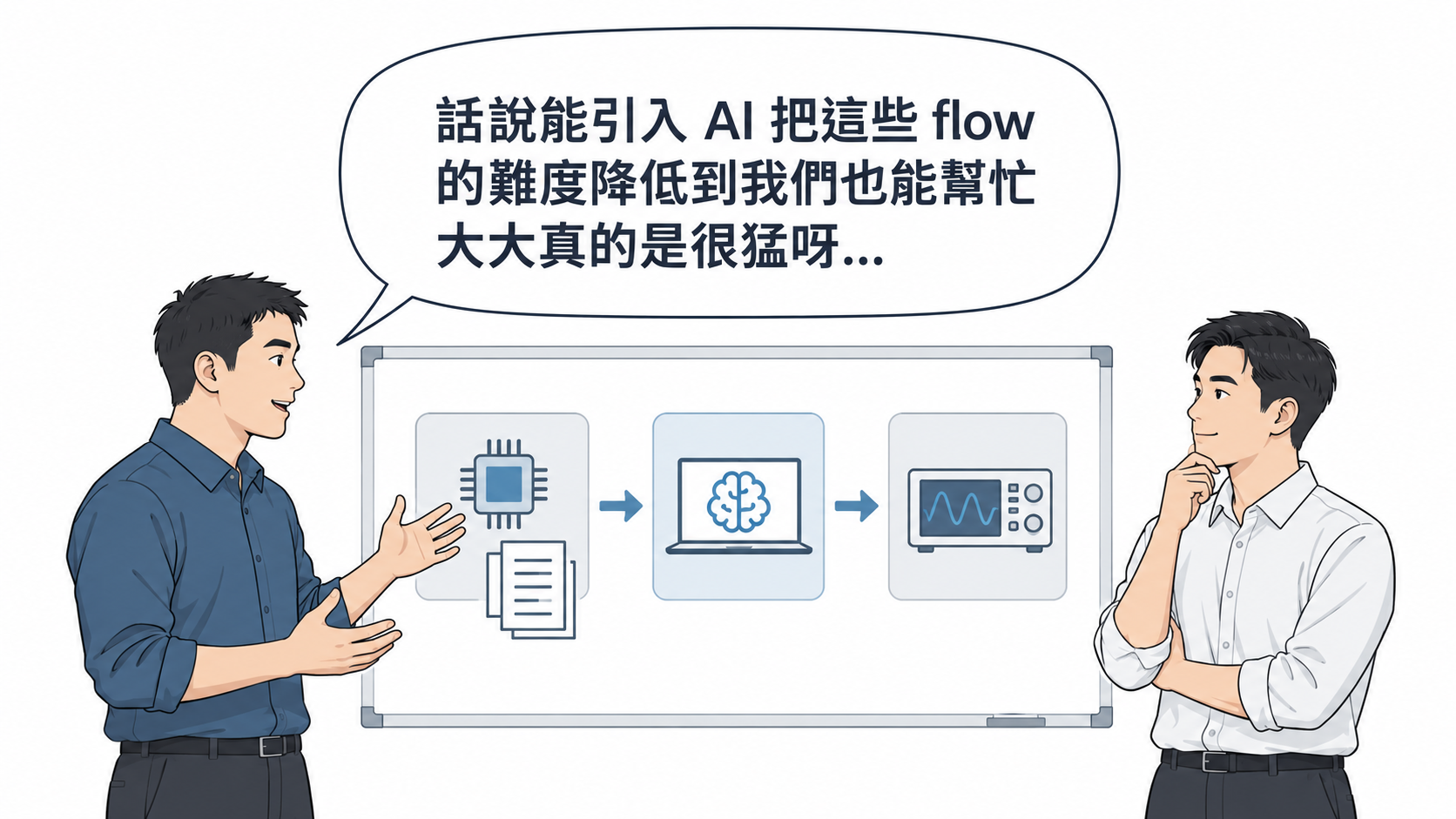
“Introducing AI lowered the difficulty of these workflows enough for us to contribute.”

Analog IC designer · October 6, 2026 · Translated from Chinese
Read the original feedback

話說能引入 AI 把這些 flow 的難度降低到我們也能幫忙

Engineers bring years of knowledge about circuits, sensors and tests. A useful AI environment gives them a more direct way to act on that knowledge, including work that crosses into software and tooling.

01 / The judgment behind the tools

I have worked across the product. That shapes how I build with AI.

My hands-on work spans ASIC architecture and circuit design, sensors, firmware and software, electronics, mechanical integration and customer support. It began with low-voltage energy-harvesting circuits, grew into ultrasonic sensing and imaging at Berkeley, and continued through product work at TDK-InvenSense and UltraSense.

Working across those boundaries taught me to follow a problem through the whole system. In a past touch-sensing analysis, some intentional presses and false triggers looked the same in the available data. The next step was to evaluate signal history and additional sensing information. The sensor, acquisition circuit, firmware and algorithm all shaped what we could learn.

I bring those dependencies into the work I give AI: the hardware state, what each data value means, the timing that matters and the evidence needed to check a change. Years of building and debugging hardware help me turn an engineering intention into a task that software can carry out.

That experience also shaped the environment I built. I connected chip knowledge to code, prepared firmware and tools in emulation before silicon arrived, and connected the software to the bench. Colleagues can turn their expertise into executable changes, then inspect the result on real hardware.

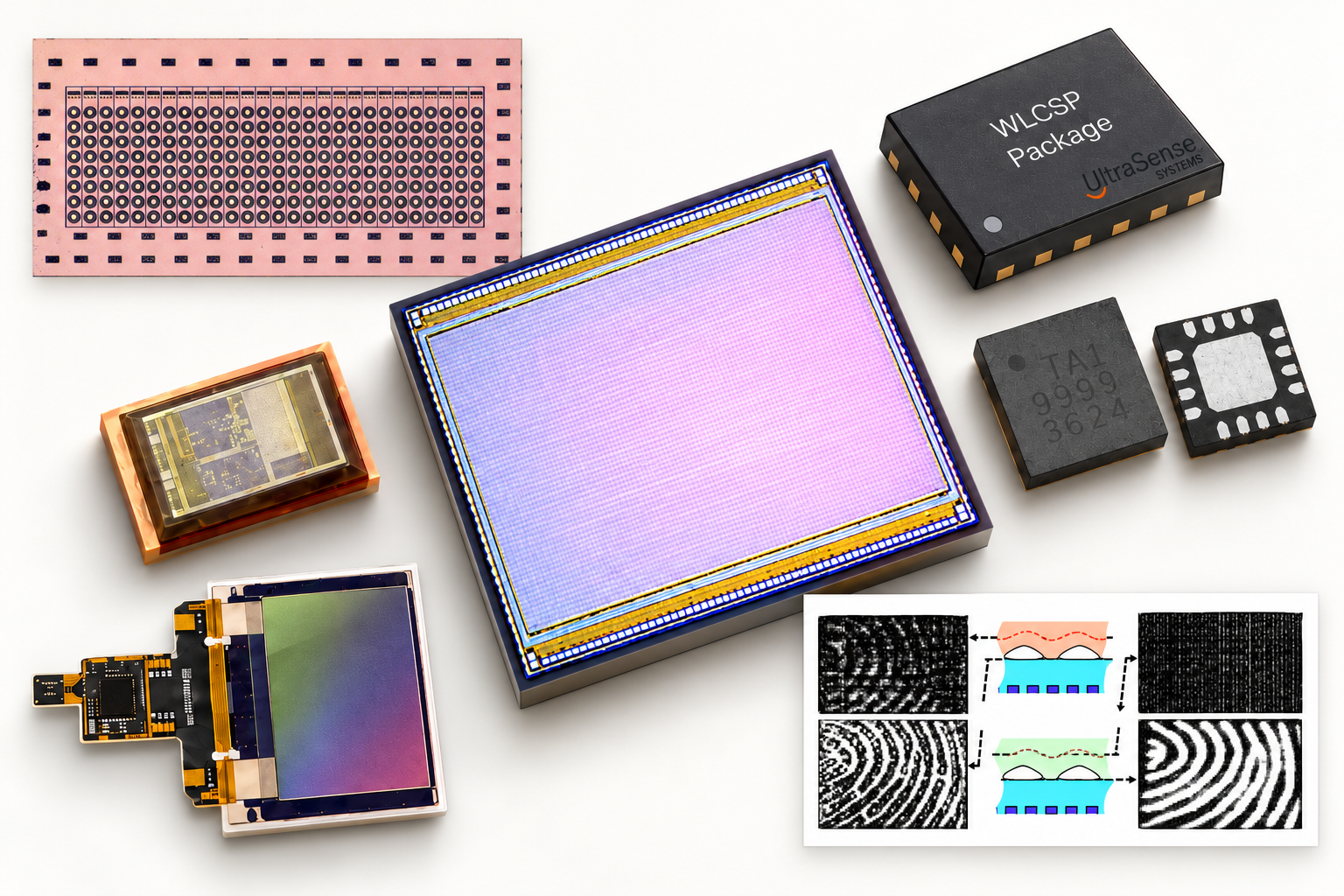
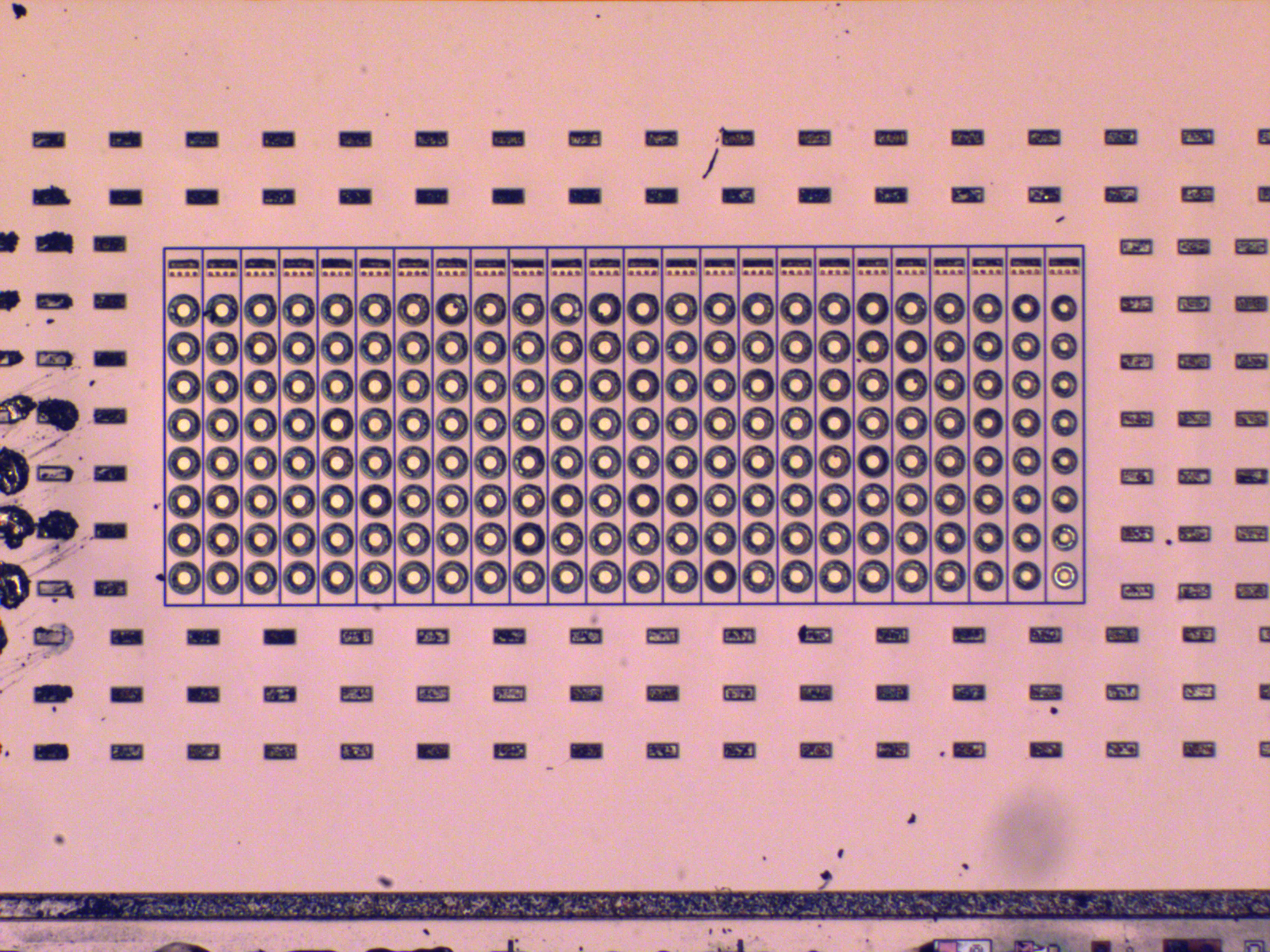
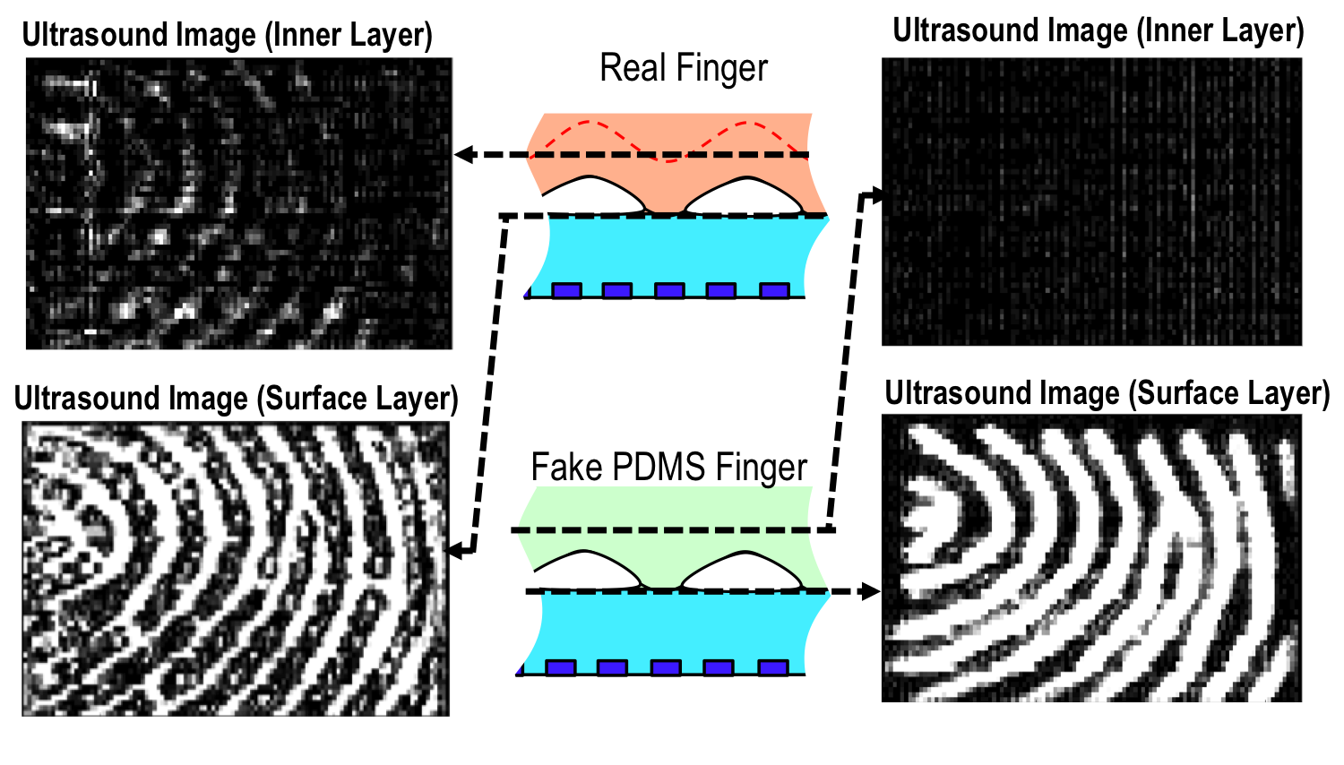
AI-assisted portfolio composition of transducer arrays, silicon dies, chip packages and ultrasonic imaging.Original PMUT array micrographPublished comparison of real-finger and PDMS-phantom surface and inner-layer ultrasound images.
Transducers, interface circuits and ultrasonic imaging—the signal-chain experience behind how I define and check AI tasks. AI-assisted portfolio composition with original research figures.

Research & original figures ↗Fingerprint imaging ↗

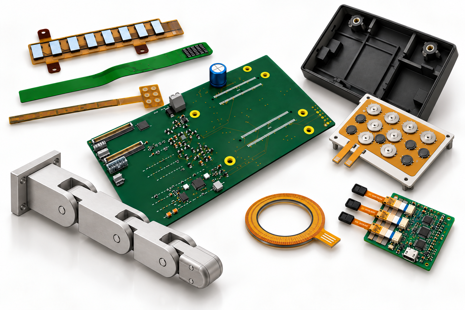
AI-assisted composition of PCB assemblies, flexible sensors, a mechanical assembly and a sensor enclosure from the existing portfolio.
Boards, flexible sensors and mechanical assemblies. Working across these interfaces helps me connect software changes to physical behavior. AI-assisted portfolio composition.

Explore the hardware portfolio ↗

02 / What I built

Chip knowledge, code and bench tools—connected for the team.

I used AI as my implementation partner to build and integrate the core environment. Each connection follows a lesson from hands-on hardware work.

01 Define the task with chip context

What hardware work taught meA register value only makes sense with the device state, timing and signal path behind it.

What I built or connectedConnect chip knowledge with firmware, software and the operating tools used to act on it.

What an engineer can doGive AI a precise change to make and the context needed to check it.

02 Prepare software before the chips arrive

What hardware work taught meFirmware and host tools can be prepared while the team waits for silicon.

What I built or connectedBuild an emulation environment to exercise firmware and related software interfaces.

What an engineer can doRun and inspect software workflows before chip delivery, then continue at the bench.

03 Make the experiment part of the workflow

What hardware work taught meA code change needs to agree with the signals and physical behavior measured on hardware.

What I built or connectedConnect firmware, Python APIs, GUIs and bench interfaces to the test workflow.

What an engineer can doRun an experiment, inspect the data and retain the useful tools for the next test.

I define and connect

Engineering judgment, core environment and integration.

AI helps implement

Code, tools, analysis and working records.

Engineers act and judge

Hardware operation, experiments, tool changes and interpretation.

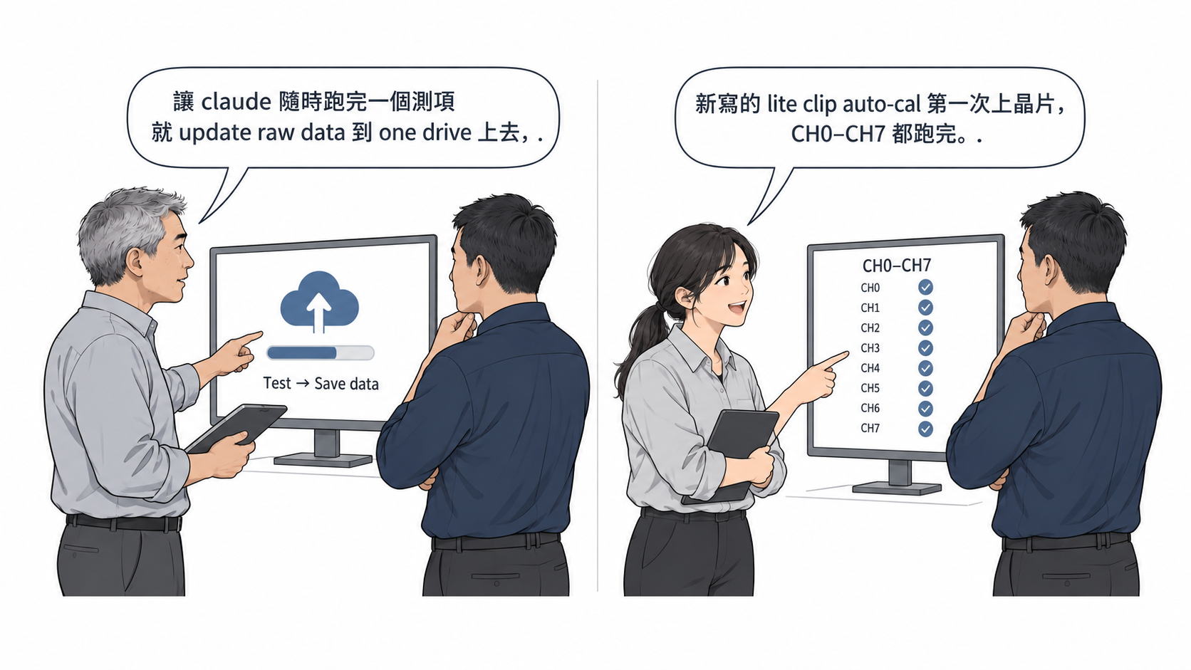
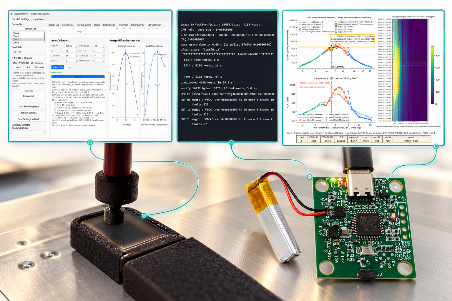
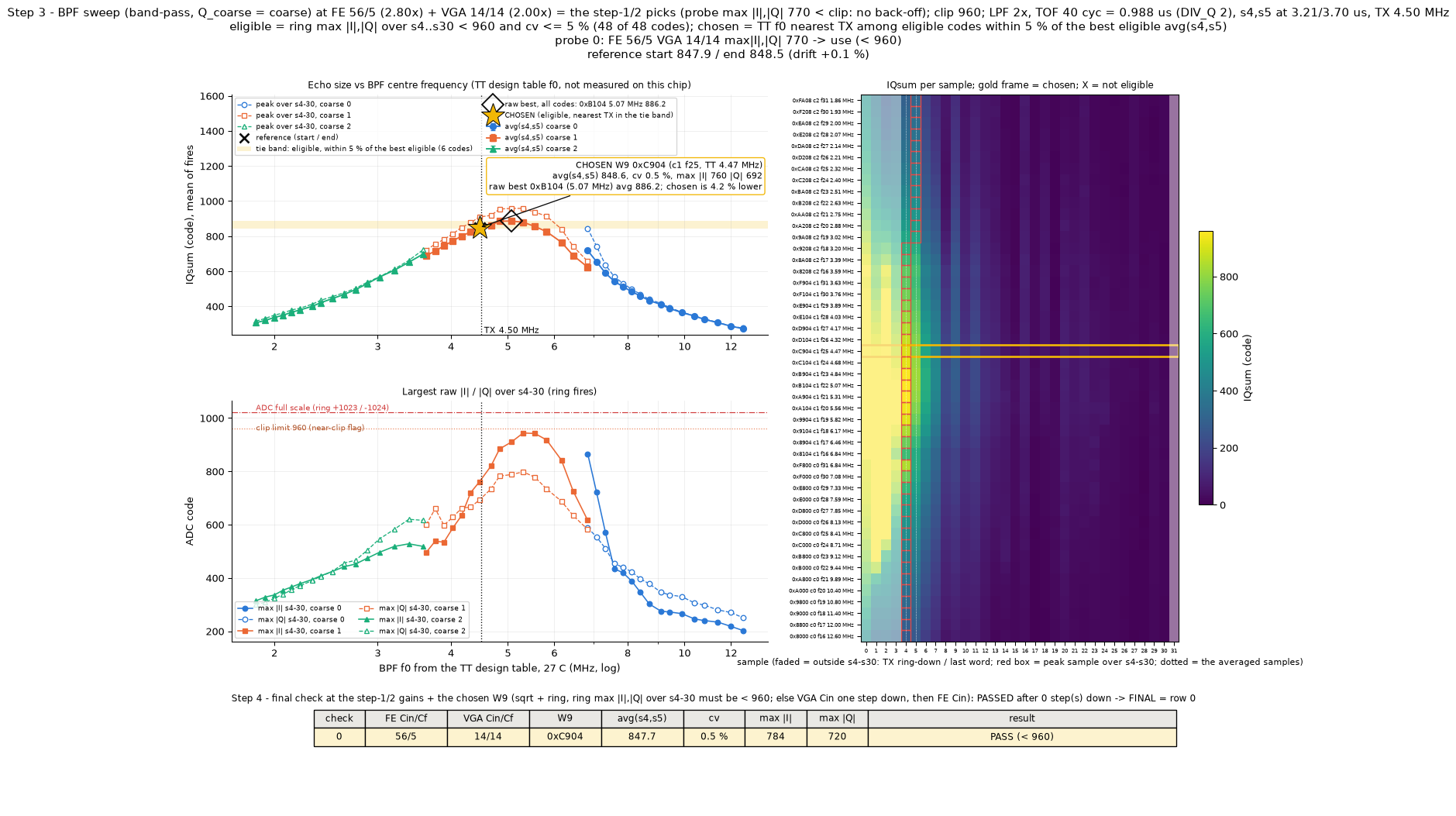
Engineering workflow composition showing original emulation software, firmware programming and calibration output above illustrated bench hardware.Original September 23 pre-silicon emulation GUI captureOriginal chip output recording firmware readback and an advancing heartbeat, with initial timeout faults also visible.Original October 7 calibration sweep and final check
Prepare the software, load firmware, inspect measurements. These original captures show separate runs along the workflow I connected for colleagues. AI-assisted composition.

Emulation ↗Firmware bring-up ↗Calibration ↗

03 / From preparation to arrival-day bring-up

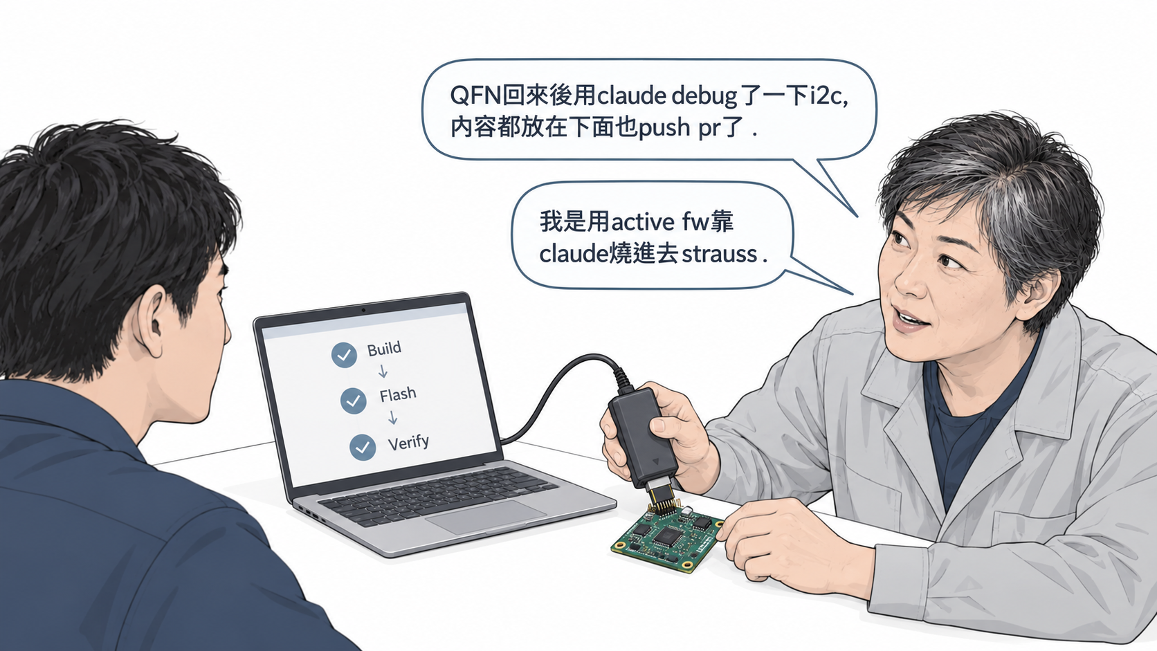
On arrival day, an analog designer began bringing up the chip with AI.

Before the new chips arrived, I used AI to prepare firmware, software tools and an emulation environment. When silicon reached the bench, an analog designer could use those tools to investigate communication, change code and load firmware.

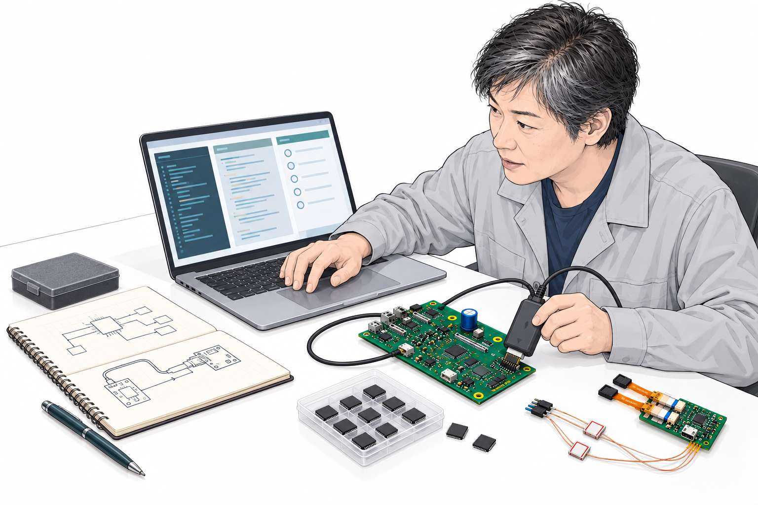
Illustrated anonymous engineer uses a laptop and programmer beside a board and a tray of chip packages.
Prepared tools in an engineer’s hands. AI illustration based on existing portfolio and feedback artwork; the original run records are shown below.

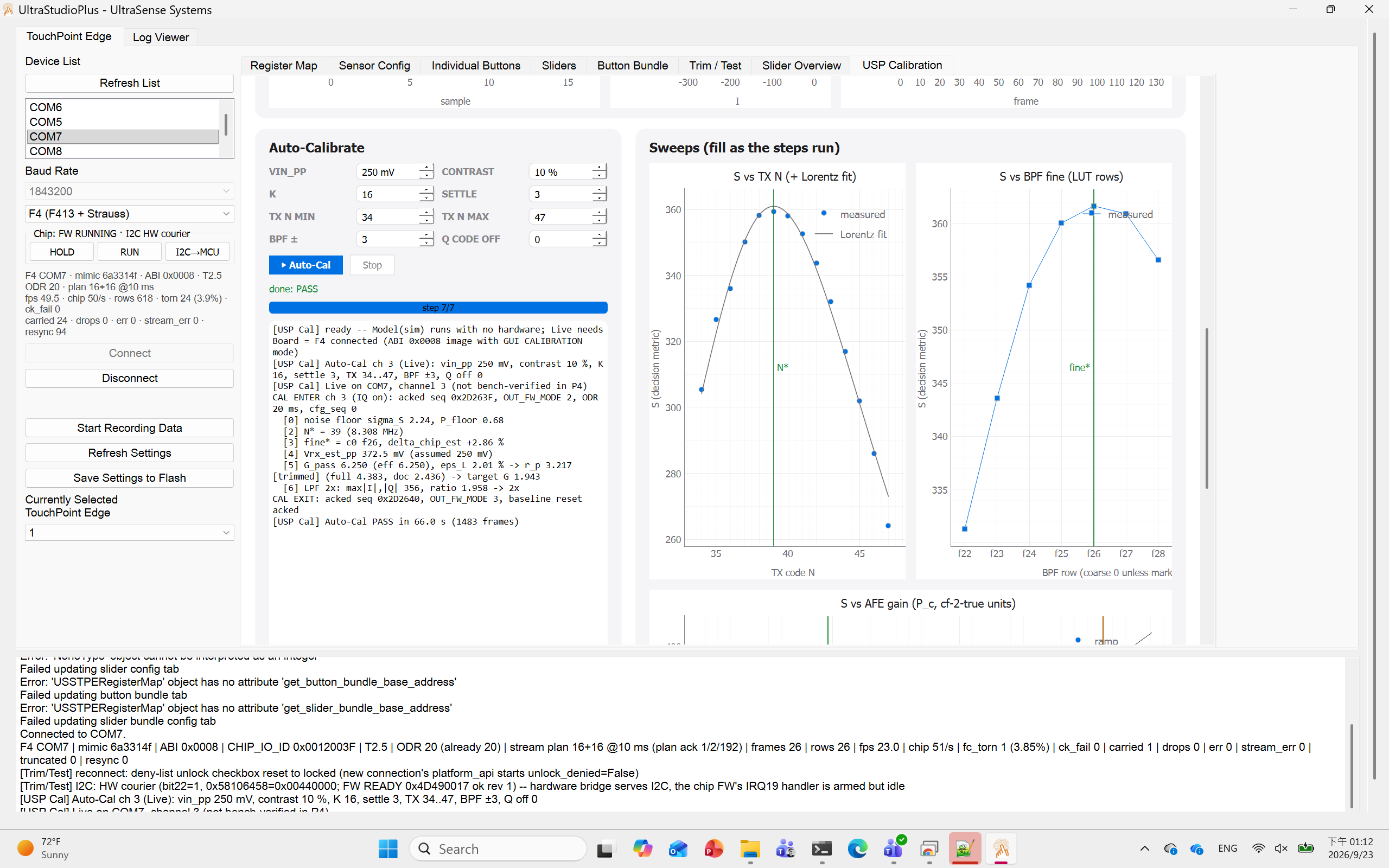
Run the calibration workflow before silicon arrives.

The September 23 emulation session exercised a calibration workflow through the software interfaces. It gave us a way to run and inspect the software before connecting it to physical silicon.

Original September 23 pre-silicon emulation GUI capture
Before silicon: the September 23 emulation GUI runs the calibration workflow. Preparing the software here gave the team tools to use when the chips arrived. Open original ↗

Debug I²C, submit a change and load firmware.

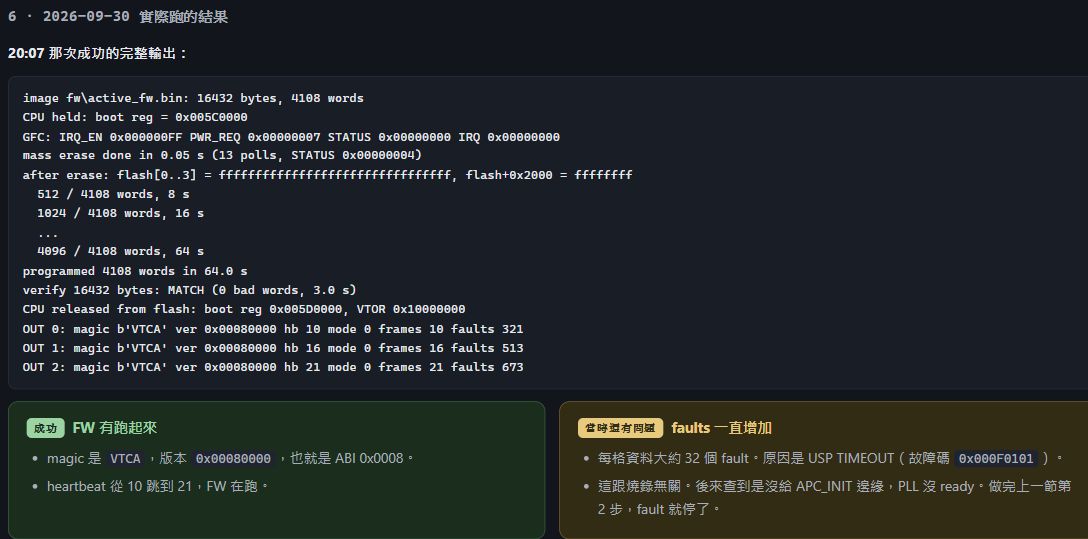
When the QFN chips arrived, an analog designer used Claude and the prepared bench tools to investigate an I²C problem. He submitted a firmware code change and reported programming active firmware into the device.

Original chip output recording firmware readback and an advancing heartbeat, with initial timeout faults also visible.
At the bench: September 30 firmware readback and an advancing heartbeat, preserved in the October 1 report. Initial faults are visible alongside the recorded output. Open original ↗

What carried into real work

An analog engineer could carry his question into a code change.

The prepared environment gave the designer a direct path from a communication problem to debugging, a firmware change and programming the device. The recorded output shows firmware readback and an advancing heartbeat. His hardware knowledge guided the work; the tools gave him a way to act on it.

This is the change I want to leave with a team: engineers can turn their judgment into executable experiments, check what happens on hardware and give the next person a useful starting point.

Read the implementation and test record

04 / Capability that keeps growing

The tools became something colleagues could adapt.

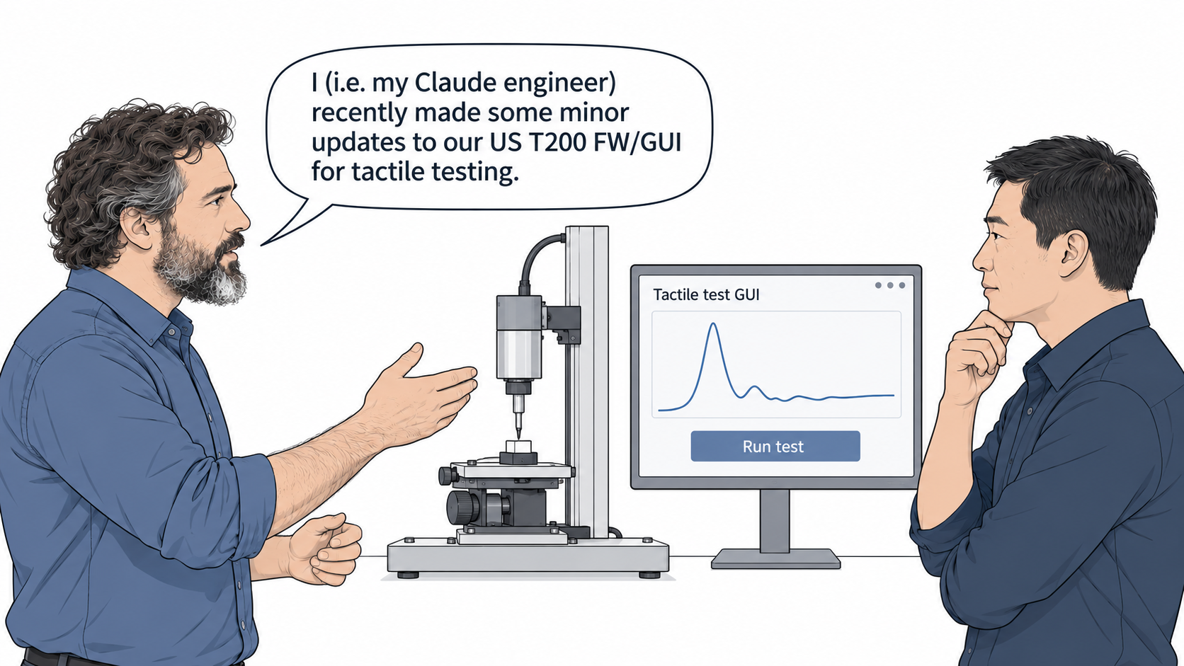
An engineer changed the firmware and GUI for his own test.

On October 13, another colleague reported using his own Claude environment to make small updates to T200 firmware and its GUI for tactile testing. He kept that environment available for future changes.

His experiment could shape the tools around it. Keeping the environment available also gave him a starting point for the next change.

Tool adaptation · illustrated workflow

Firmware
Test interface
Tactile experiment
An engineer adapts the code and interface, then uses them at the bench. Concept diagram.

See how the tools were adapted ↗

Calibration time fell from 5.7 to 1.84 seconds per point.

A calibration workflow offered another practical improvement. The team reported that much of the time per point was spent waiting on the serial connection. Keeping it open reduced the reported time from 5.7 to 1.84 seconds per point—about 3.1× faster for that workflow.

An October 15 follow-up reported 4,600 points with zero errors. The change shows how tools can improve as engineers learn where an experiment spends its time.

Time per calibration point

Before5.7 s / point
Connection kept open1.84 s / point
Reported workflow · October 14–15, 2026. Bars start at zero; shorter means less time.

Measured for this calibration workflow in the reported bench run.

See the timing and test scope ↗

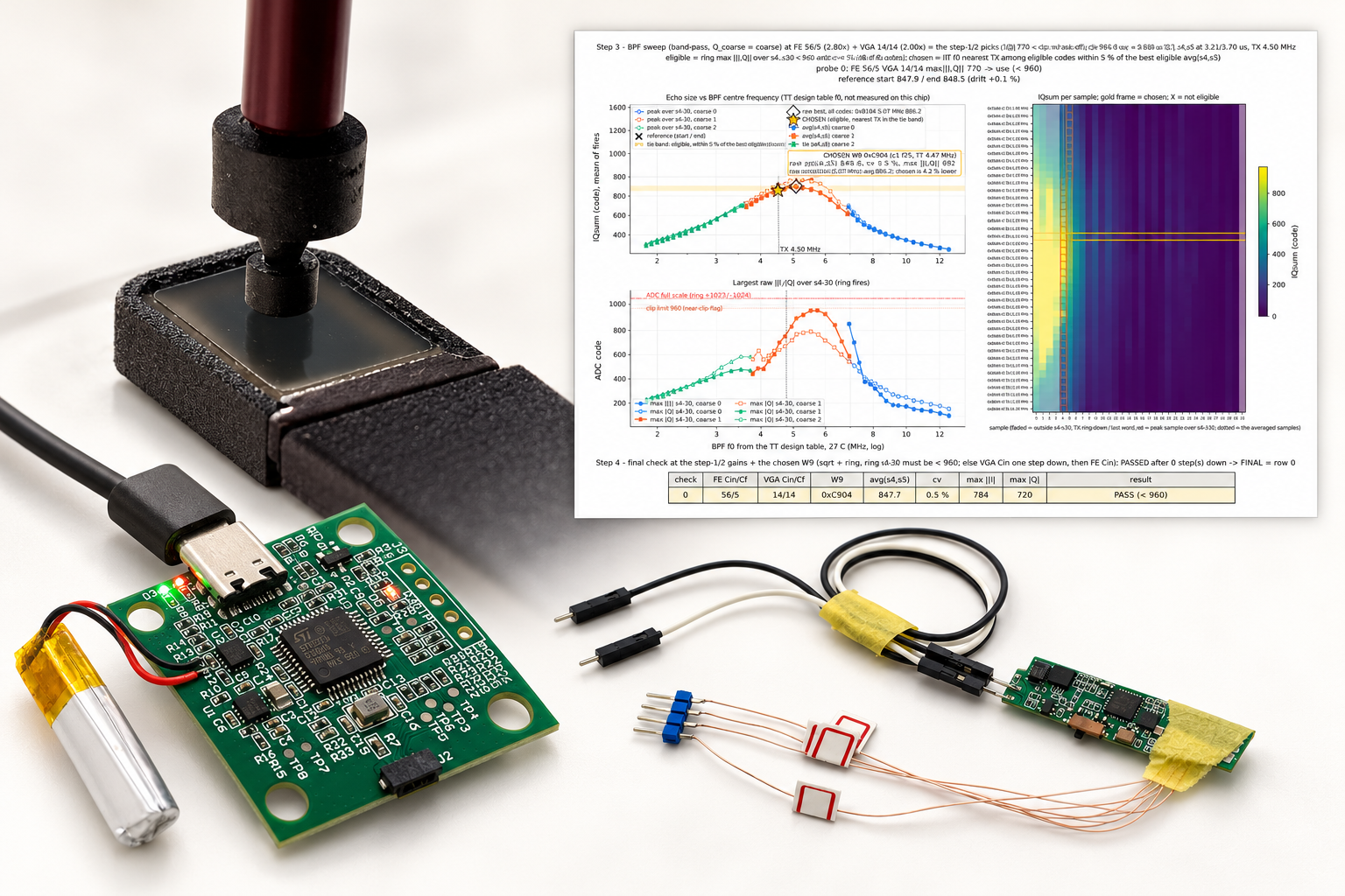
AI-assisted composition of a tactile probe experiment, development board, sensor wiring and an original calibration report.Original October 7 calibration sweep and final check
A test brings code back to the physical system. AI-assisted bench composition with the original October 7 calibration report, from a separate run to the October 14–15 timing result.

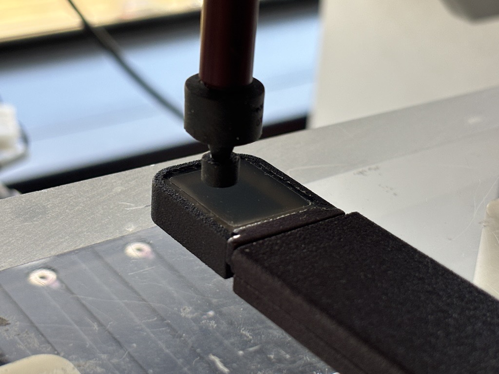
Original probe photograph ↗Original calibration report ↗

05 / The technical record

Years of building, measuring and delivering hardware.

At Berkeley, I worked across ultrasonic transducers, interface circuits and imaging. My first-author fingerprint-sensor paper received the ISSCC Lewis Winner Award for Outstanding Paper. At TDK-InvenSense and UltraSense, that work extended into hardware products and customer support. This is the foundation I bring to AI implementation: following a problem across layers and checking whether code, signals and physical behavior agree.

Published comparison of real-finger and PDMS-phantom surface and inner-layer ultrasound images.
Published ultrasonic fingerprint images: surface and inner-layer structure. JSSC 2016, Fig. 20. Open original ↗JSSC paper · Research & original figures

Follow the work in depth.

Original figures, chip designs, publications and a full career record.

Watch a touch-interface demo
An UltraSense metal-surface touch-interface demonstration. A finger presses the controls and the indicators respond.

A finger presses touch icons on a metal-surface console bar. The indicators change state as the controls are pressed.

View the demonstration still · Open the video

Work with me / Ponchi AI

Start with one useful engineering workflow.

Through Ponchi AI, I bring hardware experience and practical AI implementation to engineering teams. A useful starting point is one workflow that matters to the product: preparing for bring-up, adapting a test, analyzing measurements or helping an engineer change the tools around an experiment.

I work from your existing knowledge, code, tools and hardware constraints, build the connections the task needs, and check the result in real work. The aim is to leave your team with working tools, understandable procedures and enough context to keep improving them.
Discuss your engineering workflowExplore Ponchi AI