PONCHI AI · SPEC-TO-HARDWARE

From specs to better hardware.

AI-assisted engineering for electronics teams. Clear requirements, controlled checks and traceable results.

WORKFLOW DESIGN

From specs to hardware.

  1. Product specs

    Power, sensors, interfaces and size.

  2. AI agent

    Turn specs into design tasks.

  3. Ponchi AI

    SPICE simulation, PCB layout and enclosure CAD.

  4. AI agent

    Check results and refine the design.

  5. Hardware product

    Assembled boards, sensors and enclosures.

AI models: Anthropic · OpenAI

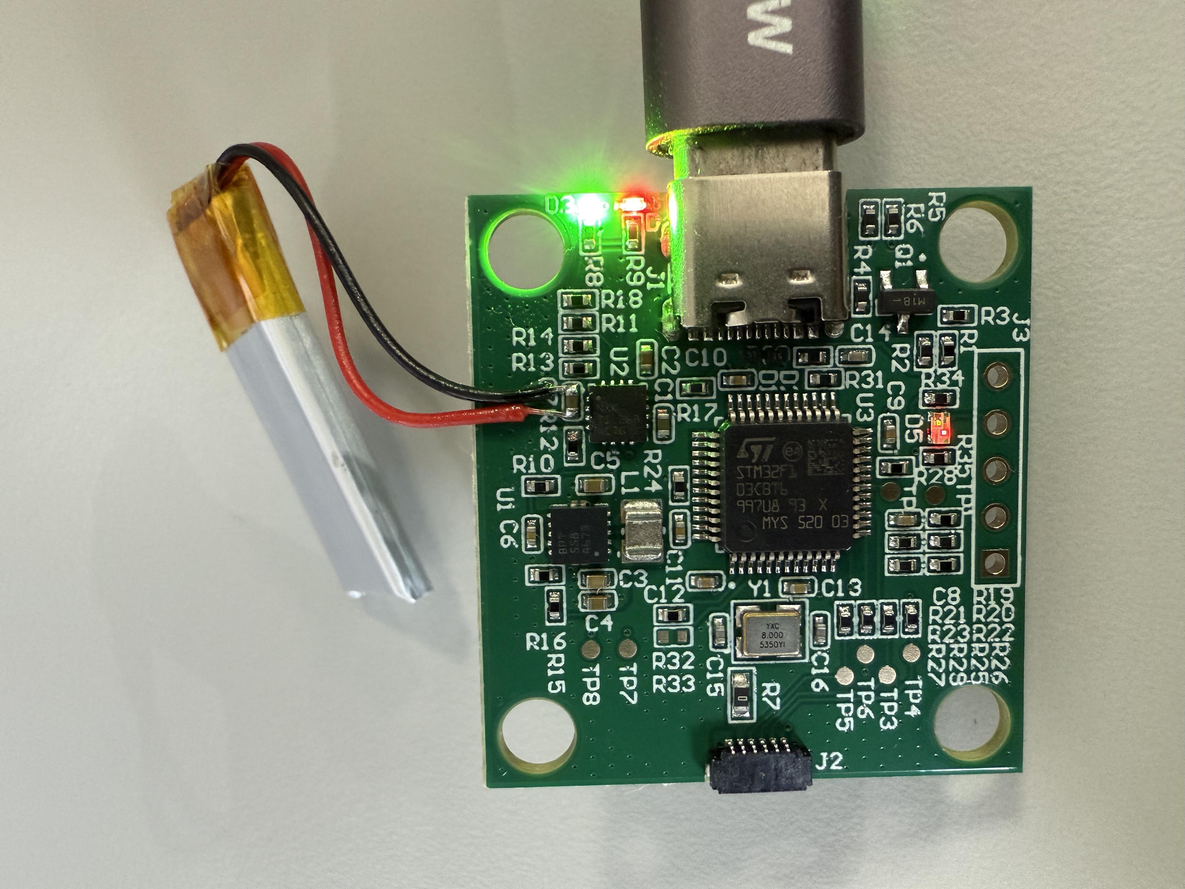
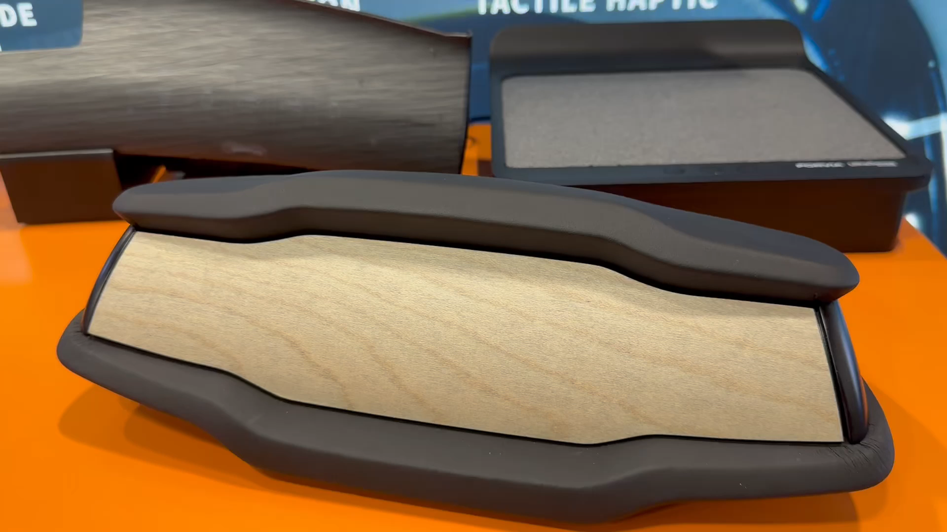
An original photograph of an UltraSense controller PCB with a battery, USB-C connection, illuminated LEDs, and surface-mount components.A shaped open-pore wood trim panel resting in its dark moulded housing on an orange surface.
Hardware examples · founder’s prior work

SPEC-TO-ASIC

Complex sensing, integrated into silicon.

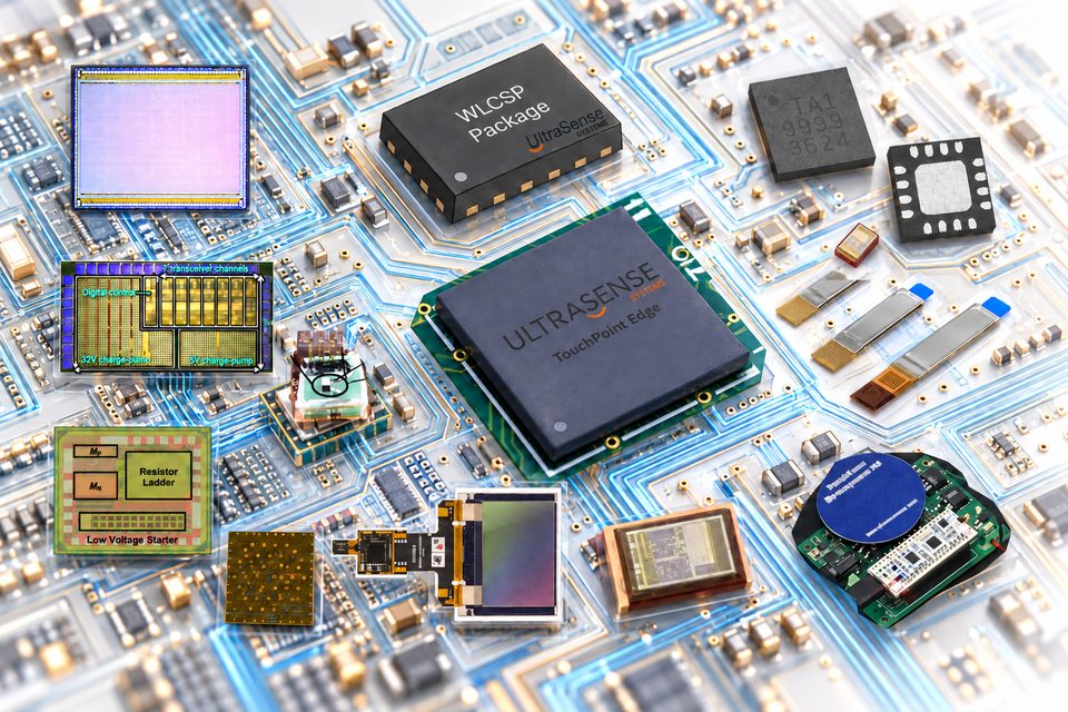
Explore our founder’s UltraSense mixed-signal ASICs and the wider chip portfolio behind them. Sensor interfaces, high-voltage drive, control and sensing algorithms come together in designs for the physical world.

An integrated AI-generated scene using the founder’s UltraSense ASIC packages, sensor modules and research die imagery, with coherent lighting and dense mixed-signal routing.
UltraSense ASICs and the founder’s silicon portfolio · AI visualization

Explore the chip portfolio

FOUNDER PRIOR WORK

AI engineering in action.

Explore the engineering work behind Spec-to-Real. These examples come from workflows our founder runs at UltraSense Systems, with design files, simulations, and tests that engineers can inspect and build on.

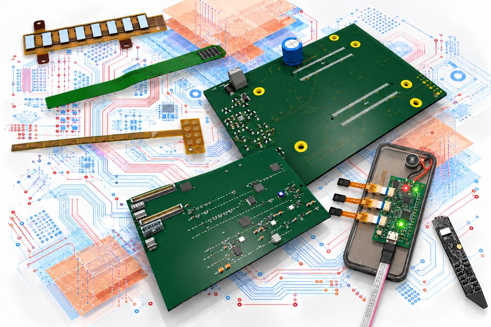
An integrated AI-generated scene based on the founder’s circuit boards and sensor FPCs, with shared lighting, connected assemblies and complex multilayer routing.
AI hardware design · boards and multilayer routing
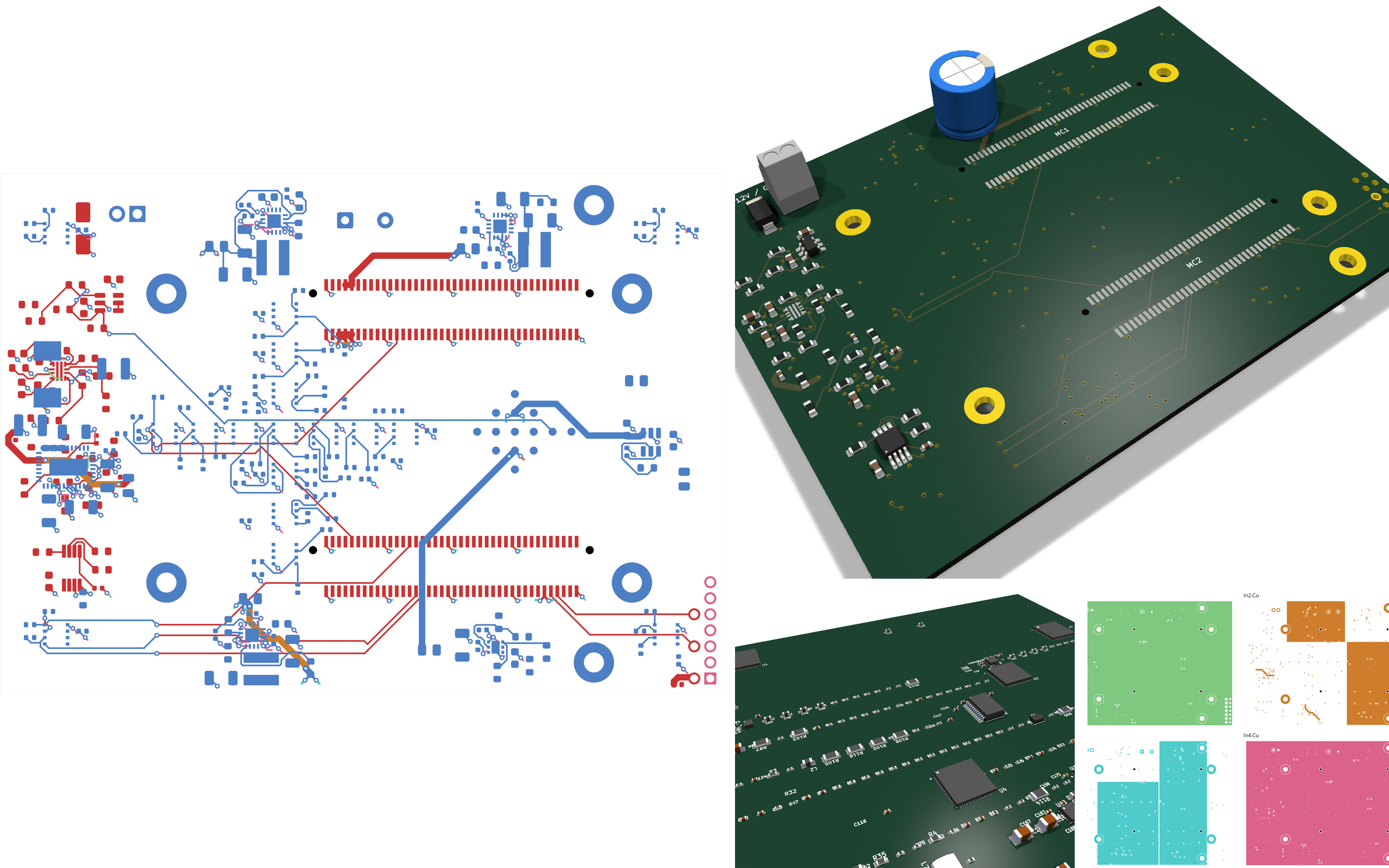
View full source imageA collage of EchoMind PCB design views: Gen2 routed copper, four internal copper layers, an isometric Gen2 view, and a close 3D view of the signal board.

Open full size

Requirements to a routed PCB

Input
Board requirements and reference designs.
Deliverables
Schematics, component placement, and routed copper.
Engineering details

The EE agent checks its choices against a reference library of 174 real board designs. Examples include an eight-channel piezo transmit-and-receive board, four-layer development kits, sensor breakouts, regulator and op-amp test boards, a reworked haptic driver stage, and a multi-channel 3D-sonar board.
Specifications to simulated analog circuits

Input
Circuit performance targets.
Deliverables
A transistor-level schematic, test bench, and simulation results.
Engineering details

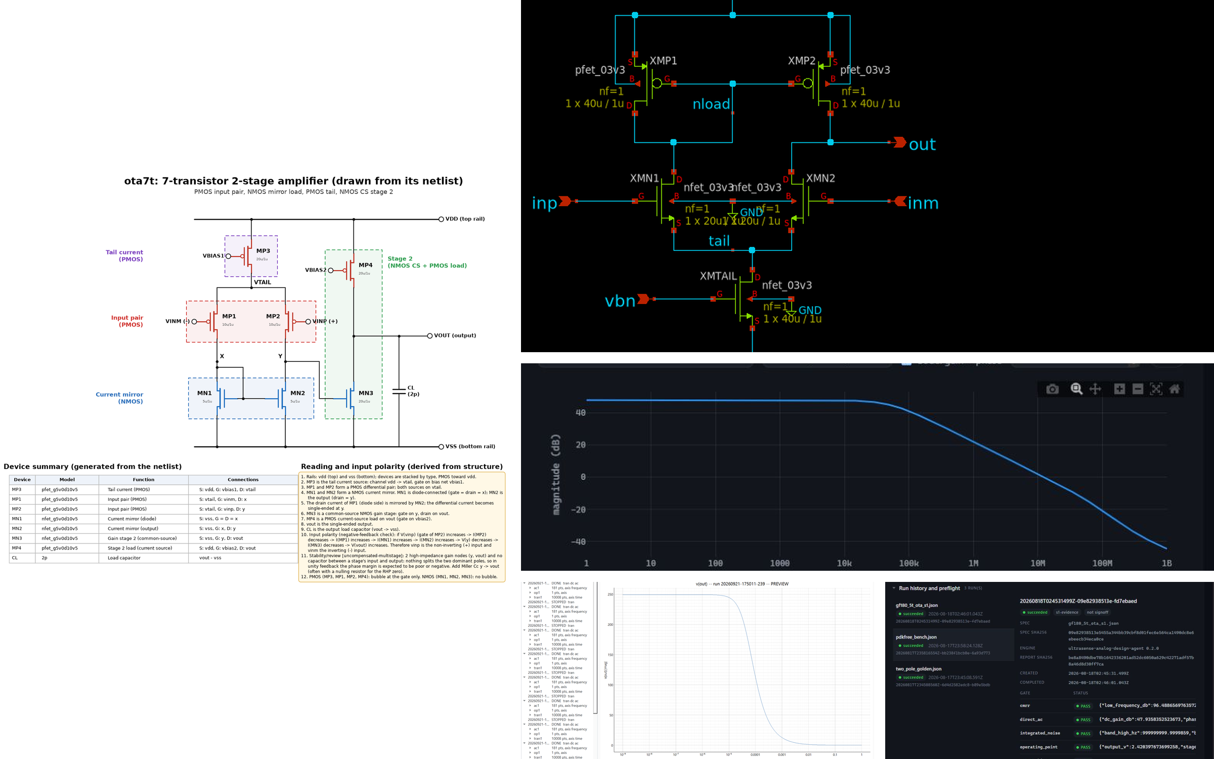
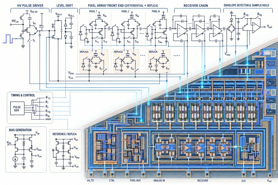
The analog agent sizes amplifier topologies from a five-transistor stage at 48 dB of gain to a folded cascode at 85 dB. Its phase margin matches Cadence Spectre to within a thousandth of a degree.

AI-generated design visualization inspired by ultrasonic analog circuits: a dense multi-stage schematic flows into a symmetric routed IC layout.
Explore circuit and simulation examples

Original transistor-level schematic

Original frequency-response example

AI analog design visualization · schematic synthesis and IC routing
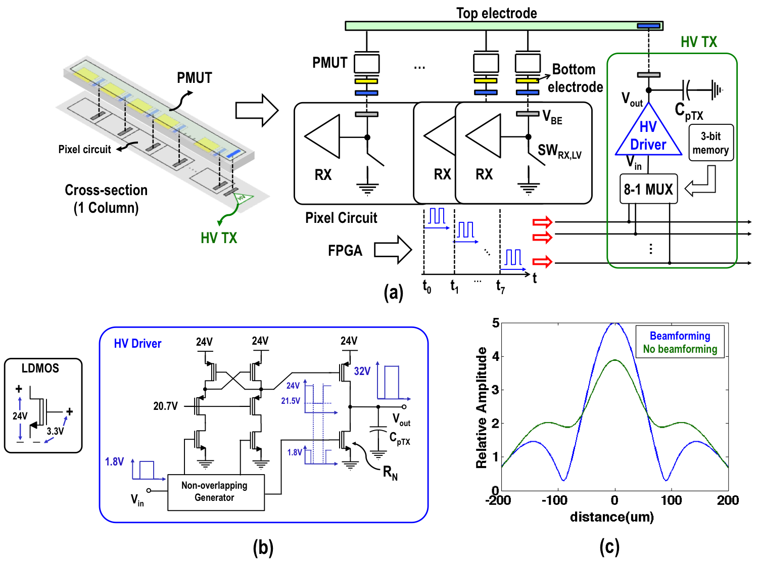
Explore the original circuit designsHigh-voltage driver from the published ultrasonic fingerprint ASIC, including the original circuit connections and annotations.

High-voltage driver · JSSC 2016, Fig. 8

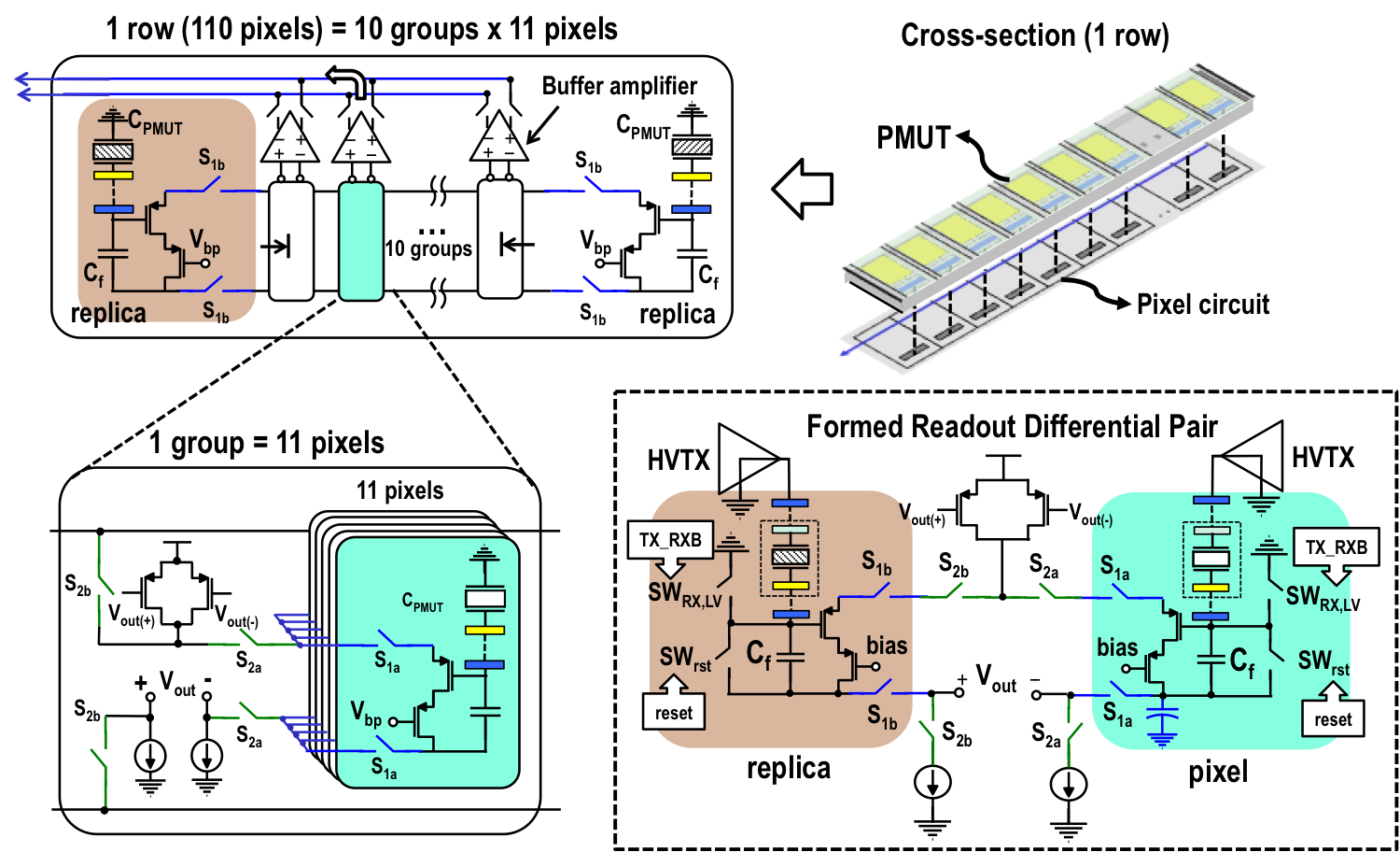
Differential pixel front-end from the published ultrasonic fingerprint ASIC, including the original circuit connections and annotations.

Differential pixel front-end · JSSC 2016, Fig. 9

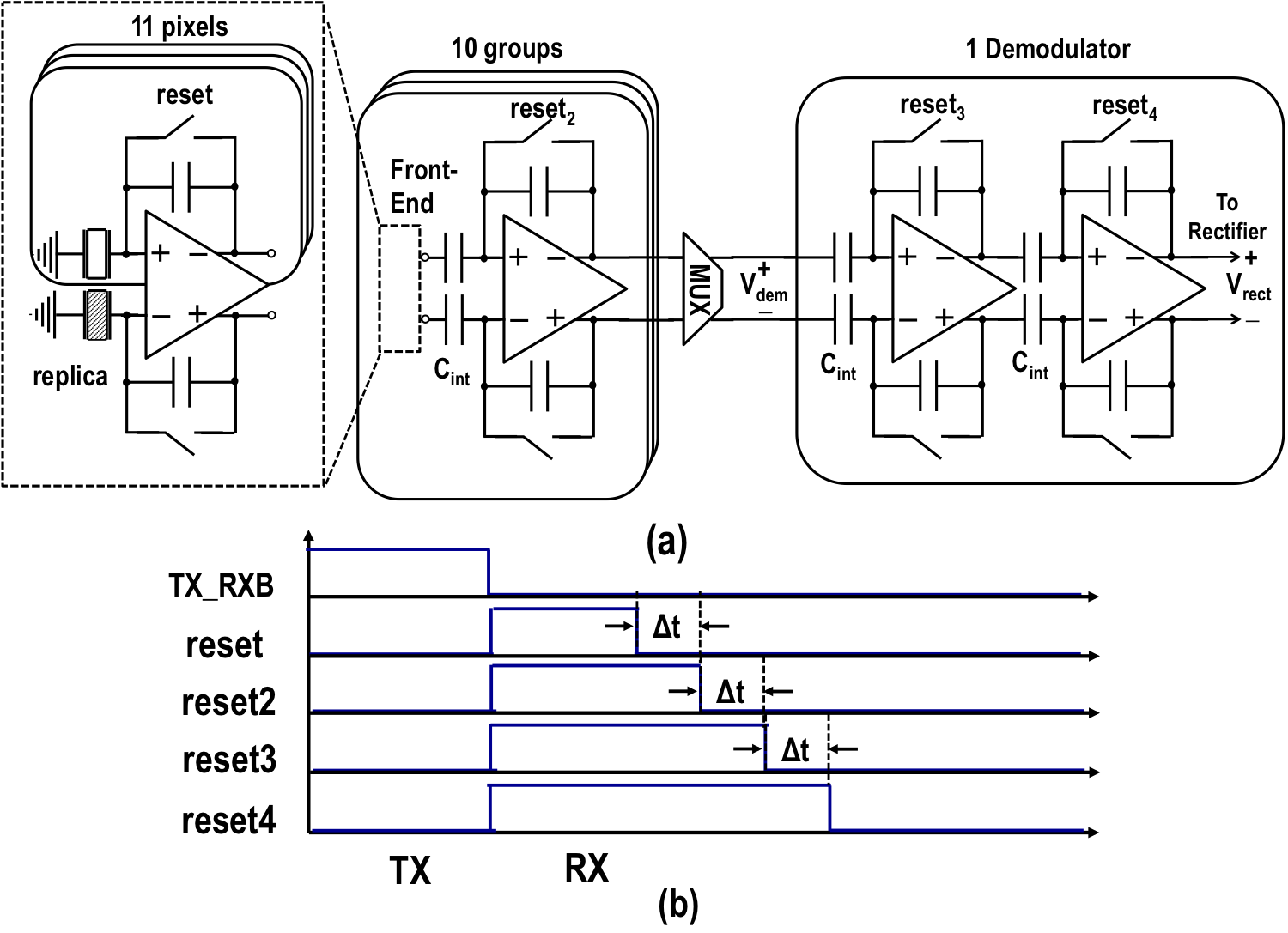
Receiver gain chain from the published ultrasonic fingerprint ASIC, including the original circuit connections and annotations.

Receiver gain chain · JSSC 2016, Fig. 11

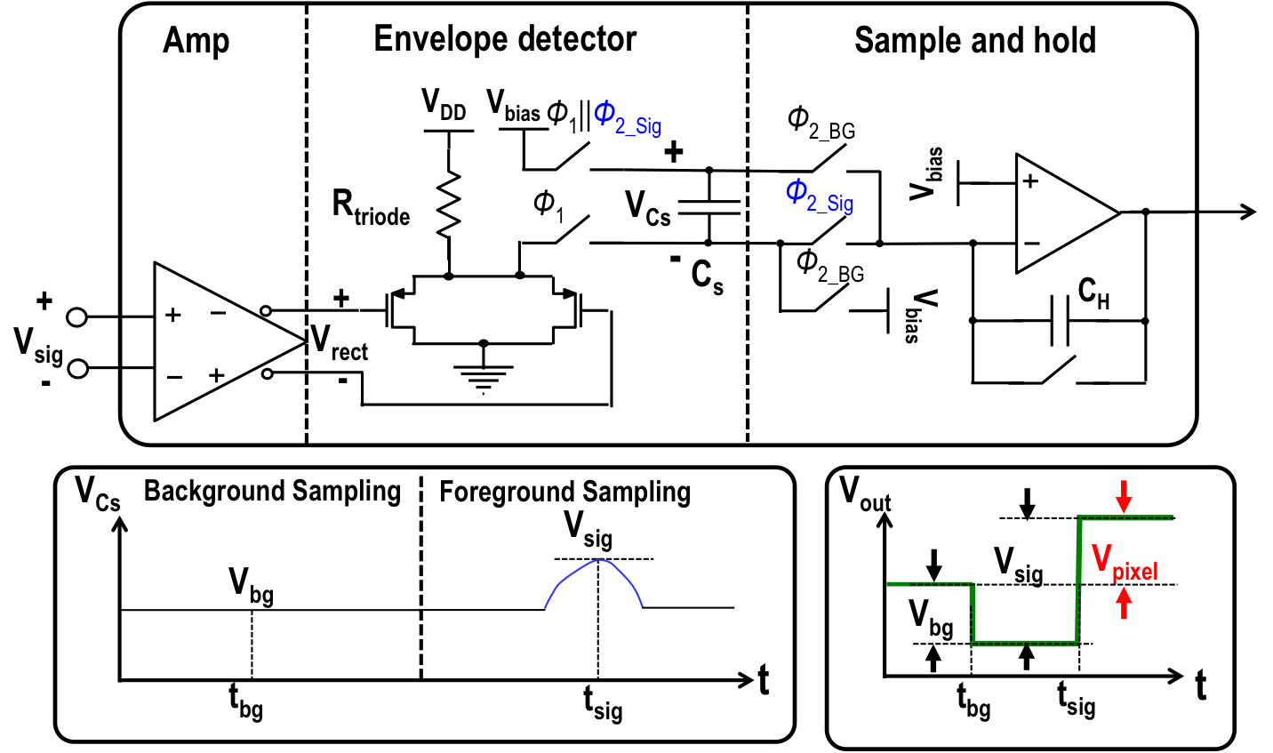
Demodulation and sample-and-hold from the published ultrasonic fingerprint ASIC, including the original circuit connections and annotations.

Demodulation and sample-and-hold · JSSC 2016, Fig. 14

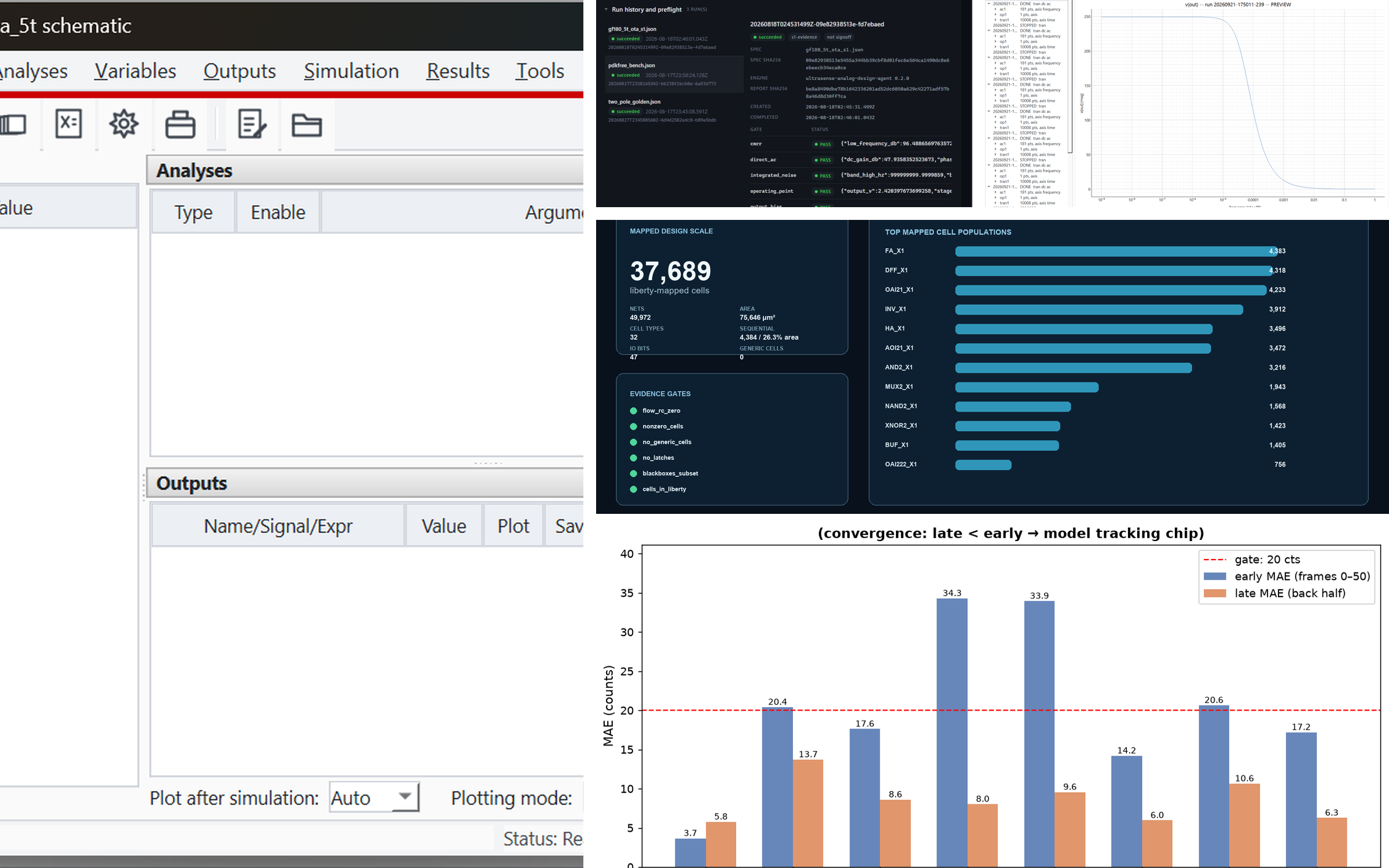
A mosaic of the analog agent's work: transistor-level amplifier schematics with device tables, frequency-response and transient plots, run-history and spec-gate screens, and its simulator workbench.

Open full size

Unchanged original subject views in one continuous presentation.
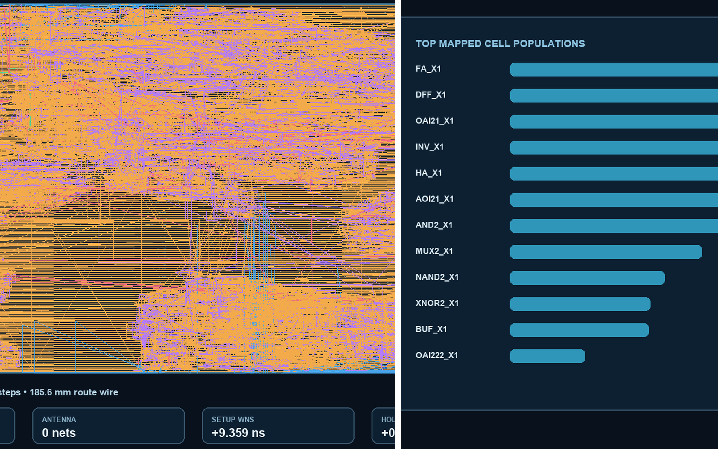
Placed-and-routed digital layout
View full source imageA placed-and-routed digital layout in orange and violet wiring beside a synthesis dashboard ranking the mapped cell populations of a 37,689-cell design.

Open full size

RTL to a routed digital layout

Input
RTL and verification requirements.
Deliverables
Verification results, synthesis, and a placed-and-routed layout.
Engineering details

A 36,000-cell design comes out placed and routed with zero routing violations, zero antenna nets, and positive setup and hold slack.

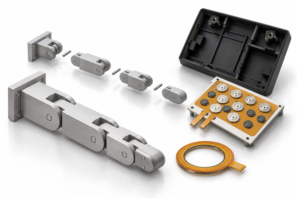
A written brief to mechanical CAD

Input
A part description and mechanical requirements.
Deliverables
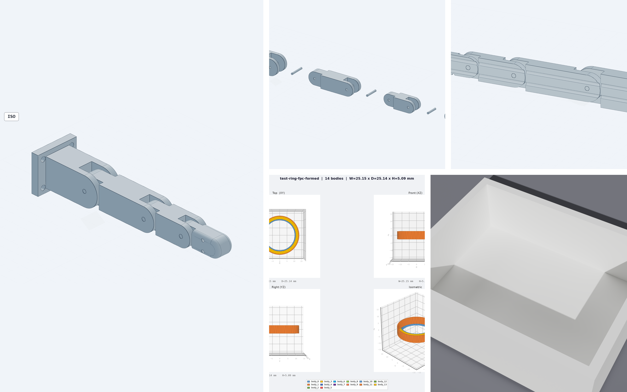
CAD models, exploded views, sections, and dimensioned drawings.
Engineering details

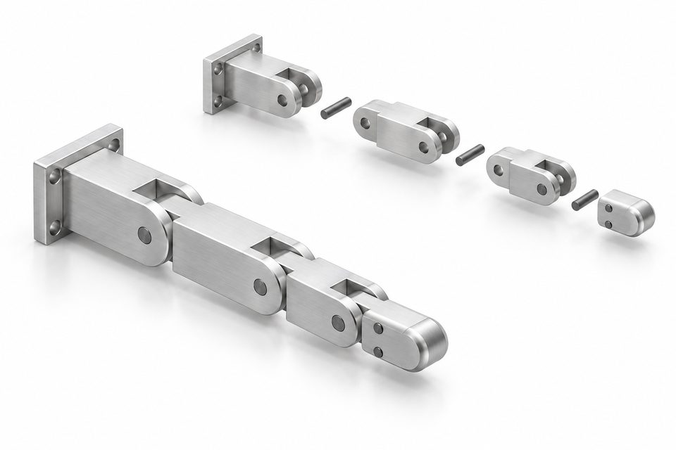
Examples include a tendon-driven robot finger, sensor evaluation cradles, test jigs, and development kit enclosures.

AI visualization combining the founder’s three-joint robotic finger CAD, exploded links, sensor-button housing and ring flex design.
Original CAD views

Original assembled CAD geometry

Original exploded components

Mechanical designs · mechanisms, housings and sensor integration · AI visualization
View full source imageA mosaic of parts the mechanical agent modelled: a tendon-driven robot finger in isometric, exploded, section, and dimensioned-drawing views, sensor cradles, a test jig, an enclosure, and a ring flex circuit.

Open full size

Styled visualization of the original three-joint robot finger geometry, with satin aluminum materials, assembled and exploded views.
Robot finger · assembly and exploded links · AI visualization
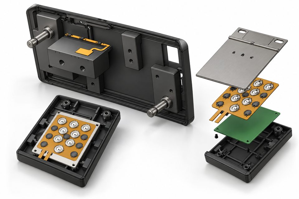
AI visualization combining original control-panel enclosure CAD with assembled and exploded sensor-button modules.
Housings, sensor mounts and exploded assemblies · AI visualization
Unchanged original subject views in one continuous presentation.
View original plots

Original recorded sensor traces and model

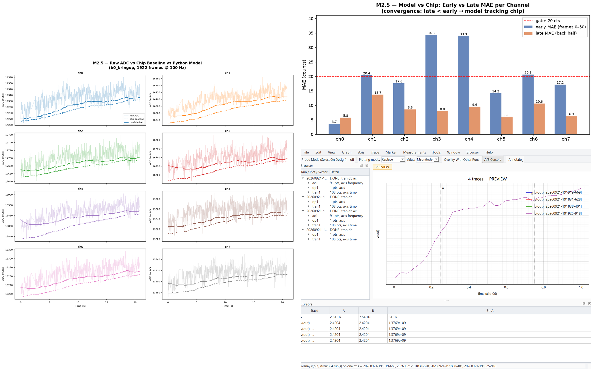
Model versus chip · per-channel error
View full source imageEight per-channel plots of recorded sensor data against the Python model, a per-channel error bar chart, and a transient overlay with measurement cursors.

Open full size

Firmware to verified sensor results

Input
Production firmware and recorded sensor captures.
Deliverables
Host execution and channel-by-channel reference comparisons.
Engineering details

Firmware runs on a host with emulated peripherals and a real I²C link. Every recorded sensor capture is checked automatically against a Python reference model, channel by channel.

FOUNDER'S SILICON WORK

A fingerprint sensor, built into silicon.

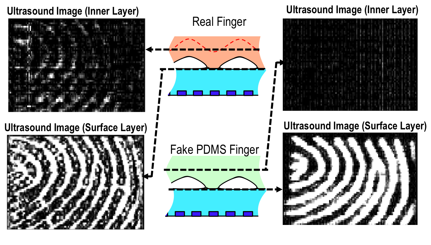
Our founder's UC Berkeley research joins ultrasonic transducers and a custom CMOS ASIC to image surface and subsurface fingerprint features. Explore the silicon and the echoes it captures.

IMAGING ASIC

Ultrasound, on a single die.

Unchanged original subject views in one continuous presentation.
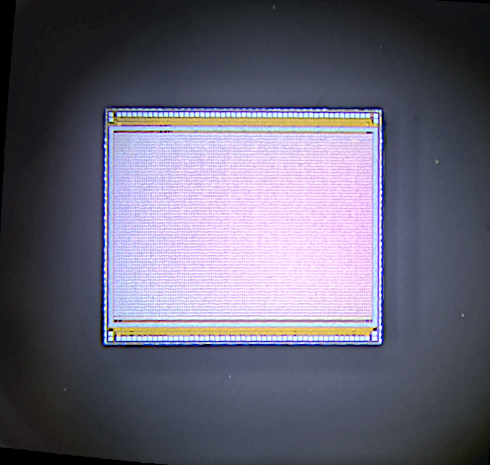
Array detailDie edge
Die size
5.36 × 4.42 mm
Front-end array
110 × 56 pixels
Readout
56 demodulators
CMOS fingerprint ASIC, before MEMS bonding.
Paper imageUnannotated original CMOS die photograph from the published UC Berkeley ultrasonic fingerprint ASIC, before MEMS bonding.

Open full image

SURFACE + SUBSURFACE

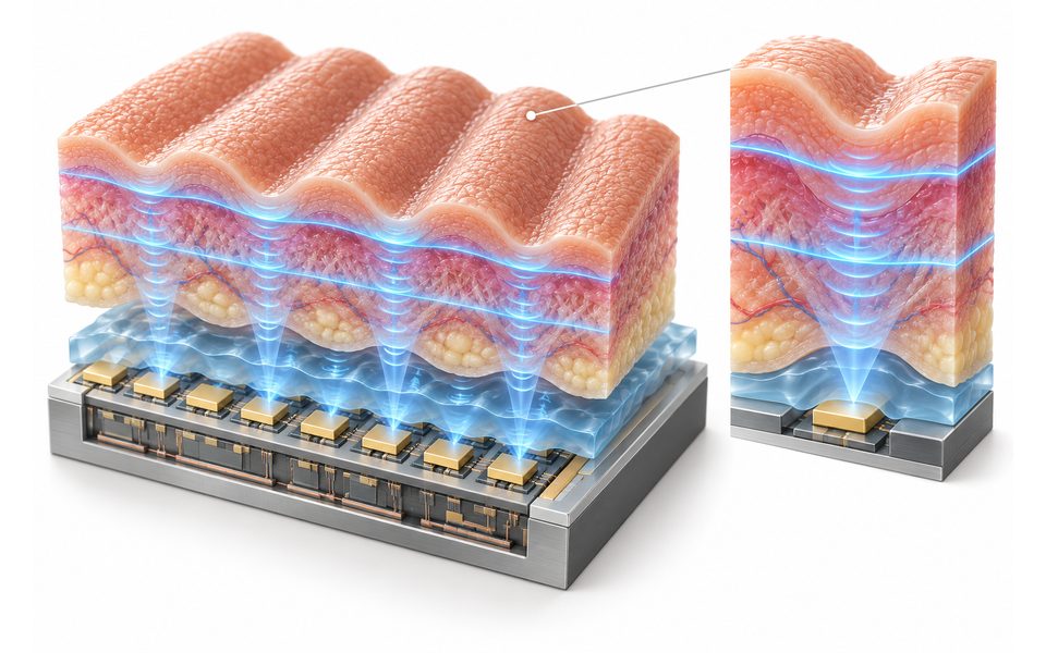
Two depths. More than a surface pattern.

Schematic illustration of ultrasonic sensing at two depths, showing tissue ridges, an acoustic transducer array, and a magnified cutaway on a continuous white background.

Schematic illustration

Real fingerPDMS replica
Surface

Real finger · surface

PDMS replica · surface

Inner layer

Real finger · inner layer

PDMS replica · inner layer

Surface and inner-layer echoes from a real finger and a PDMS replica.
Paper imagePublished ultrasonic surface and inner-layer images of a real finger and a PDMS phantom, with diagrams indicating the two imaging depths.

Open full image

Chip lead and inventor · UC Berkeley · 2012-2016

Explore the chip portfolio

THE TECHNOLOGY

AI agents connected to the tools that build things.

Model reasoning, bounded engineering tools and human review in one workflow. Explore the local requirements example and our founder's engineering methods.

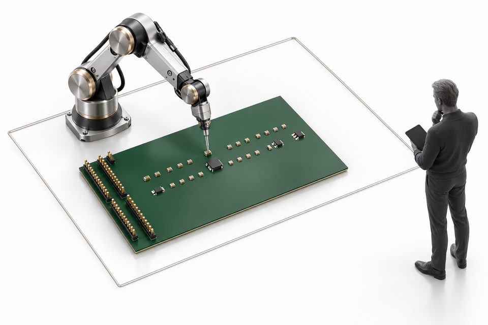
Concept illustration: a precision robot arm works inside a fine rectangular boundary while a responsible engineer stands outside with a tablet.

Delegate a bounded mission

You supply the goal, the sources, the authority, and what counts as done. The agent works inside that boundary and returns its result with the evidence attached. You delegate the task and keep the decision.

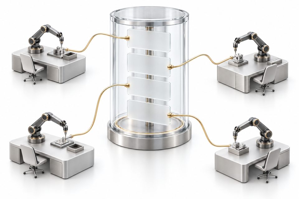
Concept illustration: four separate precision robot workstations connect to blank cards in one shared glass evidence archive.

One shared knowledge base

Agents draw on the company's own documents through retrieval rather than a model's memory, so every answer can point back to the source it came from — and several agents can work from the same ground truth.

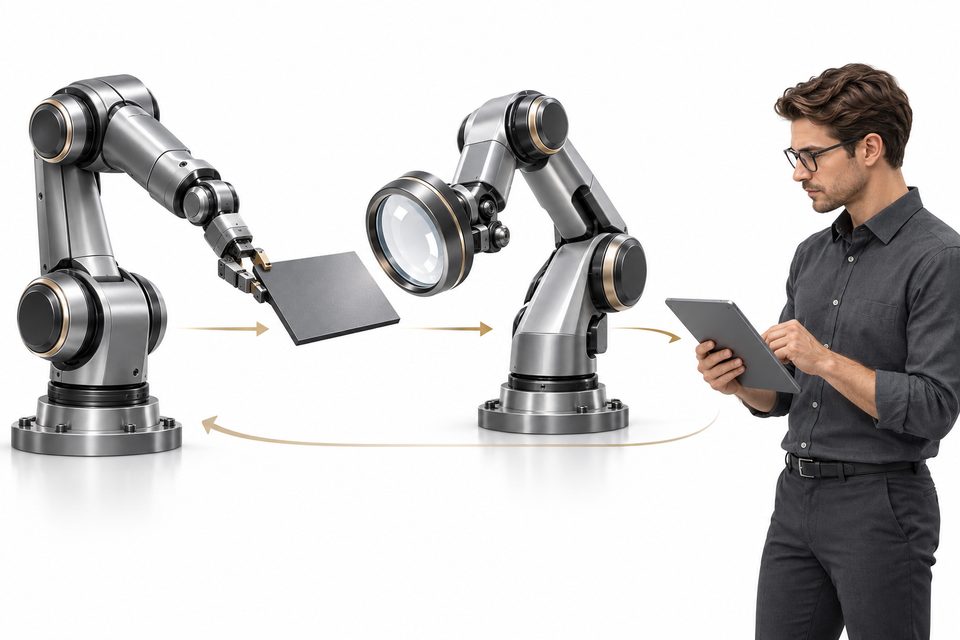
Concept illustration: a producer robot arm passes a blank design tile to an independent inspection arm, then to an engineer, with a return path for corrections.

A second agent checks the first

The agent that does the work never signs it off. An independent reviewer, starting fresh, tests the result against the acceptance criteria, and the loop repeats until the findings stop.

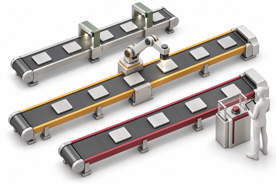
Concept illustration: three parallel workflow lanes use automatic portals, a robot reviewer, and a human release control.

Route work by consequence

Low-risk, reversible work runs with automatic checks. Work that is complex, costly to get wrong, or hard to undo gets broken down, independently reviewed, and released by a person.

IMPLEMENTATION SERVICES

Bring Spec-to-Real into your team.

Alongside product development, we provide AI consulting and implementation services. Start with an engineering workflow, connect the tools and knowledge it needs, and build a system your team can run and extend. Workshops, workflow assessment, focused builds, and training provide practical entry points.

Workshop

A half-day or full-day session for leadership and the people who do the work. What today's AI tools and agents can actually do, shown live on your kind of work, and a short list of workflows worth trying first.

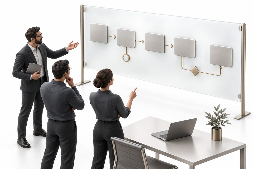
Concept illustration: a consultant and two engineers discuss blank workflow tiles connected on a frosted-glass board.

Workflow assessment

I sit with one team, map how a real piece of work moves from input to output, and mark where an agent can take a step, where a person must keep the decision, and what evidence would show it helped.

Unchanged original subject views in one continuous presentation.
Implementation report · original software capture
View full source imageA mosaic of agent software running on an engineer's computer: simulator windows, run-history and spec-gate screens, result browsers, analysis dashboards, and plots.

Open full size

Pilot build

One bounded workflow, built end to end: the agent, its tools, the knowledge it reads, and the checks around it — running on your machines, against your own data, with your team reviewing every result.

Concept illustration: four separate precision robot workstations connect to blank cards in one shared glass evidence archive.
Concept illustration · shared engineering evidence
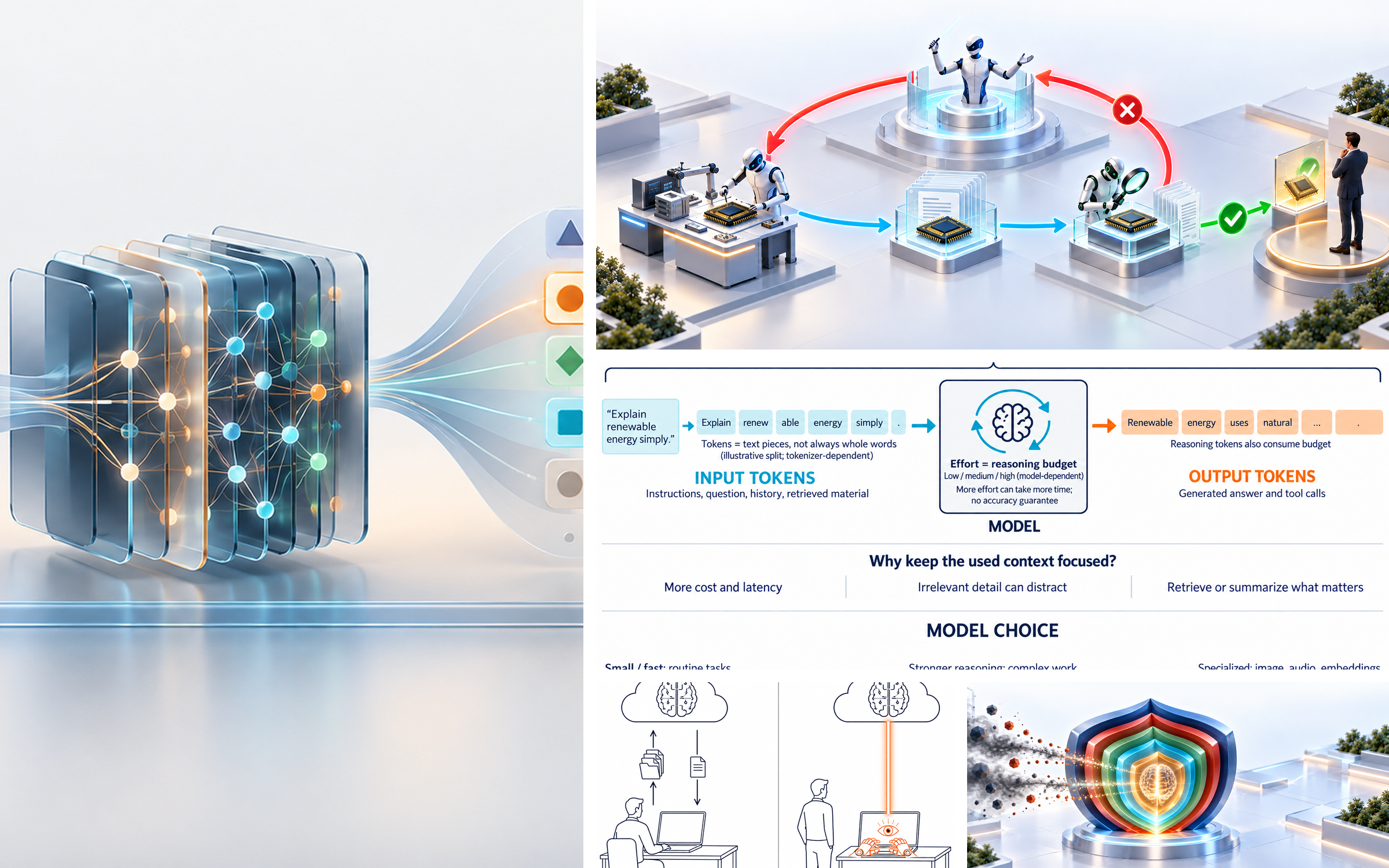
View full source imageA mosaic of training illustrations: how a model predicts tokens, the reasoning loop, the context window, the producer-and-auditor loop, and the layers that keep an agent inside its permissions.

Open full size

Implementation and training

The pilot becomes a working system your team owns. Standing instructions, shared memory, review loops, and the training that lets your people extend it without me.

Unchanged original subject views in one continuous presentation.

HOW AN ENGAGEMENT RUNS

From your specification to a checked design.

Start with the physical outcome you want to create. Each step produces engineering work you can inspect and a clear decision about the next step.

Define the physical goal

The chip, board, device, or object you want to create, with functional requirements and acceptance criteria.

01

Connect the tools and knowledge

Engineering software, reference designs, and project documents brought into a focused agent workflow.

02

Generate and verify the design

Agents produce design files and run checks, with engineers reviewing the outputs against the specification.

03

Prepare the build handoff

Organize the design outputs and verification results for the next engineering or fabrication step.

04

Integrate and train

Put the workflow in your team's hands, with instructions, review loops, and training to extend it.

05

A FATHER’S SIDE PROJECT · DRAW-TO-PLAY

It started with his daughter’s drawing.

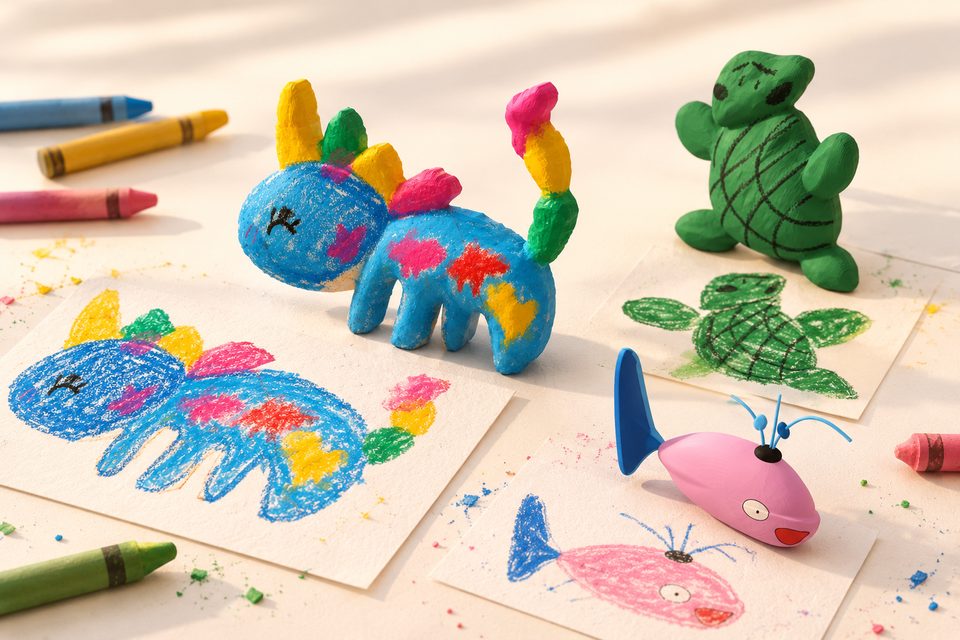
Recorded demonstration. Between chips, circuit boards, and mechanical designs, Hao-Yen spends his days building hardware with AI. Then he saw his daughter’s drawing and wanted to do something simple: make her happy.

He built an agent workflow to bring her painted characters to life — carrying their own shapes and colours into 3D designs and little animations. That family moment became Draw-to-Play, a small side business with a warm purpose: helping a child see their imagination come alive.

Meet the drawings and their characters

Warm AI visualization combining the original multicolor creature and turtle drawings with their existing 3D studies and a pink fish character.
From her drawings to characters with depth · AI visualization

ABOUT

About Ponchi AI and its founder.

Ponchi AI is an independent, early-stage AI venture founded by Hao-Yen Tang. We are developing engineering workflows for electronics teams, starting with requirements checks and traceable reports, alongside consulting and implementation work.

Company information

Location
San Jose, California
Contact email
info@ponchiai.com
Founder contact
haoyen@ponchiai.com

I'm Hao-Yen Tang, co-founder and CTO of UltraSense Systems, where I run chip, firmware, algorithm, and system engineering. I work on the same problem from both ends: the physics of a piezoelectric transducer, and the mixed-signal circuit that has to read it for microamps in a car door at minus forty degrees.

Before UltraSense I was a staff IC designer at TDK-InvenSense, where I was chip lead across several generations of the UltraPrint ultrasonic fingerprint sensor family. I did my PhD at UC Berkeley in Bernhard Boser's group, where the fingerprint sensor-on-a-chip I built became the prototype for that product line and won the 2016 ISSCC best paper award.

Over the past year I have put AI agents to work across my company's engineering — chip design, firmware, test, documentation — and learned what it takes for a team to trust what they produce. Through Ponchi AI, I develop Spec-to-Real AI services that connect specifications and designs to chips, boards, and physical objects. Alongside that product work, I help engineering teams build agent workflows and train the people who run them.

Company information and product work

3,223

citations

29

h-index

36

granted US patents

Citation figures from Google Scholar, as of 2026-10-08.

Recognition

ISSCC BEST PAPER

Lewis Winner Award for Outstanding Paper

IEEE International Solid-State Circuits Conference, 2016 · for “3D Ultrasonic Fingerprint Sensor-on-a-Chip”

The chip in that paper became the prototype for a commercial ultrasonic fingerprint sensor product line.

3 papers at ISSCC

IEEE International Solid-State Circuits Conference, the venue where new chip designs are first presented

2014, 2015, 2016

Predoctoral Achievement Award

IEEE Solid-State Circuits Society

2015

Outstanding Student Paper Award

IEEE International Conference on Micro Electro Mechanical Systems

2017

CHIP PORTFOLIO

Ten chip programs, from thesis to production.

Explore Hao-Yen Tang's chip work across ultrasonic fingerprint imaging, touch and force sensing, medical ultrasound, and energy harvesting. Each program shows the device, his role, and the papers or patents behind it.

UltraPrint ultrasonic fingerprint sensor family

MASS PRODUCTION

TDK-InvenSense · 2016-2018 · mobile and automotive

Piezoelectric micromachined ultrasonic transducers built monolithically on CMOS: the sensor, its analog front end, and an MCU on one die. The imaging chain reads a fingerprint through glass and metal by transmit beamforming and pulse-echo timing.

Chip lead, multiple generations · mixed-signal front end, high-voltage pulser, system bring-up

Unchanged original subject views in one continuous presentation.

TouchPoint Z

MASS PRODUCTION

UltraSense Systems · automotive

An ultrasound touch and force controller that turns an ordinary surface into a button. Sensor, analog front end, MCU, and the sensor-fusion algorithm all live on one chip, so a button can be placed behind metal with no hole and no moving part.

Chip lead · architecture, mixed-signal front end, high-voltage pulser, on-chip sensing algorithm

TouchPoint Edge

SAMPLING

UltraSense Systems · automotive

A multi-modal human-machine-interface SoC: capacitive touch, ultrasound touch and slider, and piezoelectric force sensing, fused on-chip. One part replaces the controller, the discrete force front ends, and the glue between them.

Chip lead · architecture, mixed-signal front end, high-voltage drive, sensor fusion

UltraClear lens-cleaning ASIC

PROTOTYPE

UltraSense Systems · automotive

A controller that keeps a camera lens clear by driving it ultrasonically. One chip carries the power conversion from the vehicle battery, the piezo driver, an on-chip Hall-effect current sensor that tracks the transducer's resonance, and the digital control.

Chip lead · architecture, piezo driver, on-chip current sensing

Ultrasonic rangefinder

MASS PRODUCTION

TDK-Chirp Microsystems · IoT

A time-of-flight rangefinder on a chip, small enough and low-power enough to sit in a consumer device. Precision frequency demodulation and low-jitter time measurement are what make a centimetre-scale echo readable at microwatt power.

Analog designer, prototype and first production generation · high-voltage pulser, PLL and frequency demodulation, mixer and filter design

Unchanged original subject views in one continuous presentation.
Array detailDie edge

3-D ultrasonic fingerprint sensor-on-a-chip

RESEARCH

UC Berkeley · 2012-2016 · productized

The thesis chip. A PMUT array bonded to CMOS that images a fingerprint in three dimensions, including the ridge structure below the skin surface. It became the prototype for a commercial fingerprint sensor product line.

Chip lead and inventor · array and circuit co-design, high-voltage pulser, beamforming

High-efficiency piezo pulser with integrated charge pump

RESEARCH

UC Berkeley · 2013-2015 · medical and fitness

A handheld, battery-powered ultrasound imager demonstrated at ISSCC. The interesting part is the drive side: getting enough voltage into a discrete piezo element from a battery, efficiently enough that the whole instrument runs at milliwatts.

Chip lead · high-voltage drive, integrated charge pump

Neural Dust piezo implant ASIC

RESEARCH

UC Berkeley · 2013-2016 · neural interfaces

A millimetre-scale implant that records neural activity and is powered and read out by ultrasound through tissue, with no battery and no wire. I built the ASIC the prototype used; the work went on to seed iota Biosciences.

ASIC provider · ASIC design, ultrasound wireless power transfer

50 mV-input batteryless boost converter

RESEARCH

National Taiwan University · 2011-2013 · energy harvesting

A DC-DC converter that starts up from 50 mV with no battery and no external kick, turning the few tens of millivolts a thermoelectric generator produces into a usable supply rail. My first silicon, and still my second most-cited paper.

Chip lead · converter architecture, startup circuit

3D Sonic fingerprint sensor

MASS PRODUCTION

Qualcomm · mobile

A large-area ultrasonic fingerprint sensor built on a thin-film transistor backplane with a piezoelectric polymer film, driven by a companion ASIC.

Analog designer · high-voltage drive, transmit beamforming

A control with no hole, no bezel and no moving part.
Stone, and the buttons are underneath it.
Unchanged original subject views in one continuous presentation.
The whole controller -- sensing, front end, MCU, algorithm.
Unchanged original subject views in one continuous presentation.

All programs

CONTACT

Discuss your project.

Tell us your goal, what you have today, and the engineering workflow you want to improve. Whether it is a chip, a board, a device, or a creative object, email us to start the conversation.

Email info@ponchiai.com