CV

Curriculum vitae

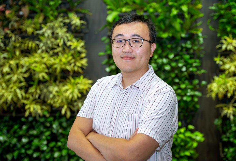
Hao-Yen Tang in a striped shirt with his arms folded, photographed smiling against a wall of green planting.

I'm Hao-Yen Tang, co-founder and CTO of UltraSense Systems, where I run chip, firmware, algorithm, and system engineering. I work on the same problem from both ends: the physics of a piezoelectric transducer, and the mixed-signal circuit that has to read it for microamps in a car door at minus forty degrees.

Before UltraSense I was a staff IC designer at TDK-InvenSense, where I was chip lead across several generations of the UltraPrint ultrasonic fingerprint sensor family. I did my PhD at UC Berkeley in Bernhard Boser's group, where the fingerprint sensor-on-a-chip I built became the prototype for that product line and won the 2016 ISSCC best paper award.

Over the past year I have put AI agents to work across my company's engineering — chip design, firmware, test, documentation — and learned what it takes for a team to trust what they produce. Ponchi AI, my consulting practice, brings that to other companies: I help leaders pick the workflows worth automating, build the agent systems that run them, and train the people who keep them running.

EXPERIENCE

Experience

Co-founder, CTO and VP Engineering, UltraSense Systems

Founded the company to commercialise an ultrasound sensor SoC that turns an ordinary surface into a touch interface. I run engineering: silicon, firmware and software, sensing algorithms, sensor and module design, mechanical, and the R&D that feeds them.

  • Mixed-signal ASIC architecture with MEMS, analog front end, and MCU on the same die
  • System hardware, module products, and board design
  • Firmware, embedded software, and sensing algorithms
  • Sensor design across acoustic, mechanical, and capacitive domains

2018–present

Staff IC Designer, TDK-InvenSense

Led a multi-disciplinary system team for the next-generation ultrasonic fingerprint sensor: bring-up, sensor calibration, and operation. Coordinated acoustics, MEMS, CMOS, firmware, and software into one solution.

2017–2018

Senior IC Designer, TDK-InvenSense

Core analog IC designer for the ultrasonic fingerprint sensor product.

2016–2017

Graduate Student Researcher, University of California, Berkeley

Bernhard Boser's group. Three ISSCC chips: an in-air ultrasonic gesture recogniser that became the prototype for Chirp Microsystems, a battery-powered handheld ultrasound imager, and the PMUT fingerprint sensor-on-a-chip that became a commercial product line.

2012–2016

EDUCATION

Education

Ph.D., Electrical Engineering and Computer Sciences

University of California, Berkeley · Bernhard Boser's group. Thesis work on piezoelectric micromachined ultrasonic transducers and the integrated circuits that drive and read them, culminating in a 3-D ultrasonic fingerprint sensor-on-a-chip.

2012–2016

B.S., Electrical Engineering

National Taiwan University

2007–2011

AWARDS

Awards

Lewis Winner Award for Outstanding Paper

IEEE International Solid-State Circuits Conference · for “3D Ultrasonic Fingerprint Sensor-on-a-Chip”

2016

Predoctoral Achievement Award

IEEE Solid-State Circuits Society

2015

Outstanding Student Paper Award

IEEE International Conference on Micro Electro Mechanical Systems

2017

SILICON

Ten chip programs, from thesis to production.

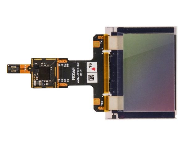
A fingerprint sensor module on a black flexible circuit, the sensor die at one end and its connector tail at the other.

UltraPrint ultrasonic fingerprint sensor family

MASS PRODUCTION

TDK-InvenSense · 2016-2018 · mobile and automotive

Piezoelectric micromachined ultrasonic transducers built monolithically on CMOS: the sensor, its analog front end, and an MCU on one die. The imaging chain reads a fingerprint through glass and metal by transmit beamforming and pulse-echo timing.

Chip lead, multiple generations · mixed-signal front end, high-voltage pulser, system bring-up
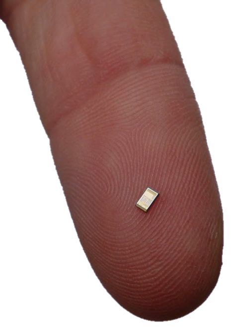
Extreme macro of a small surface-mount sensor chip resting on a fingertip.

TouchPoint Z

MASS PRODUCTION

UltraSense Systems · automotive

An ultrasound touch and force controller that turns an ordinary surface into a button. Sensor, analog front end, MCU, and the sensor-fusion algorithm all live on one chip, so a button can be placed behind metal with no hole and no moving part.

Chip lead · architecture, mixed-signal front end, high-voltage pulser, on-chip sensing algorithm

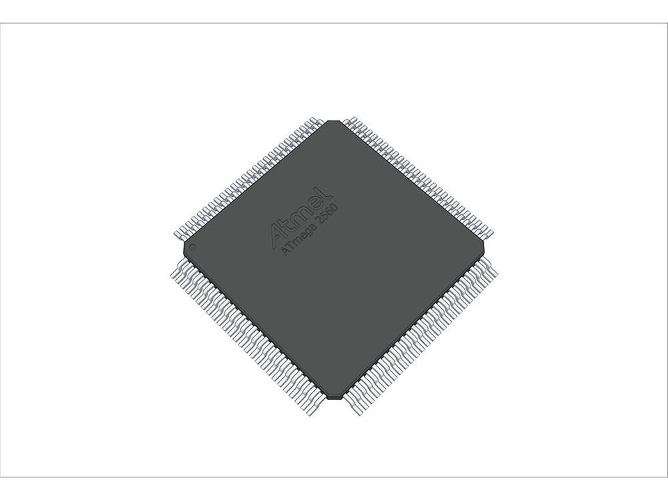
A rendering of a dark square quad-flat package with fine leads on all four sides.

TouchPoint Edge

SAMPLING

UltraSense Systems · automotive

A multi-modal human-machine-interface SoC: capacitive touch, ultrasound touch and slider, and piezoelectric force sensing, fused on-chip. One part replaces the controller, the discrete force front ends, and the glue between them.

Chip lead · architecture, mixed-signal front end, high-voltage drive, sensor fusion

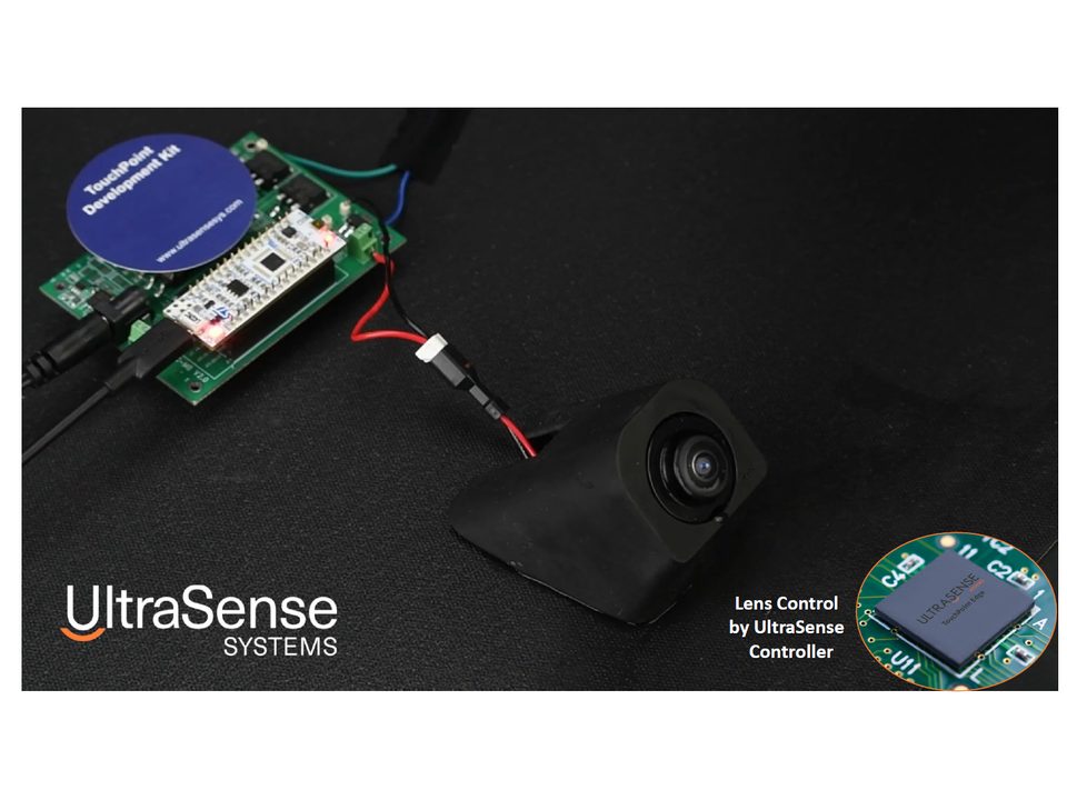
The UltraClear prototype board: a green controller board wired to a camera lens module with its piezo cleaning ring.

UltraClear lens-cleaning ASIC

PROTOTYPE

UltraSense Systems · automotive

A controller that keeps a camera lens clear by driving it ultrasonically. One chip carries the power conversion from the vehicle battery, the piezo driver, an on-chip Hall-effect current sensor that tracks the transducer's resonance, and the digital control.

Chip lead · architecture, piezo driver, on-chip current sensing

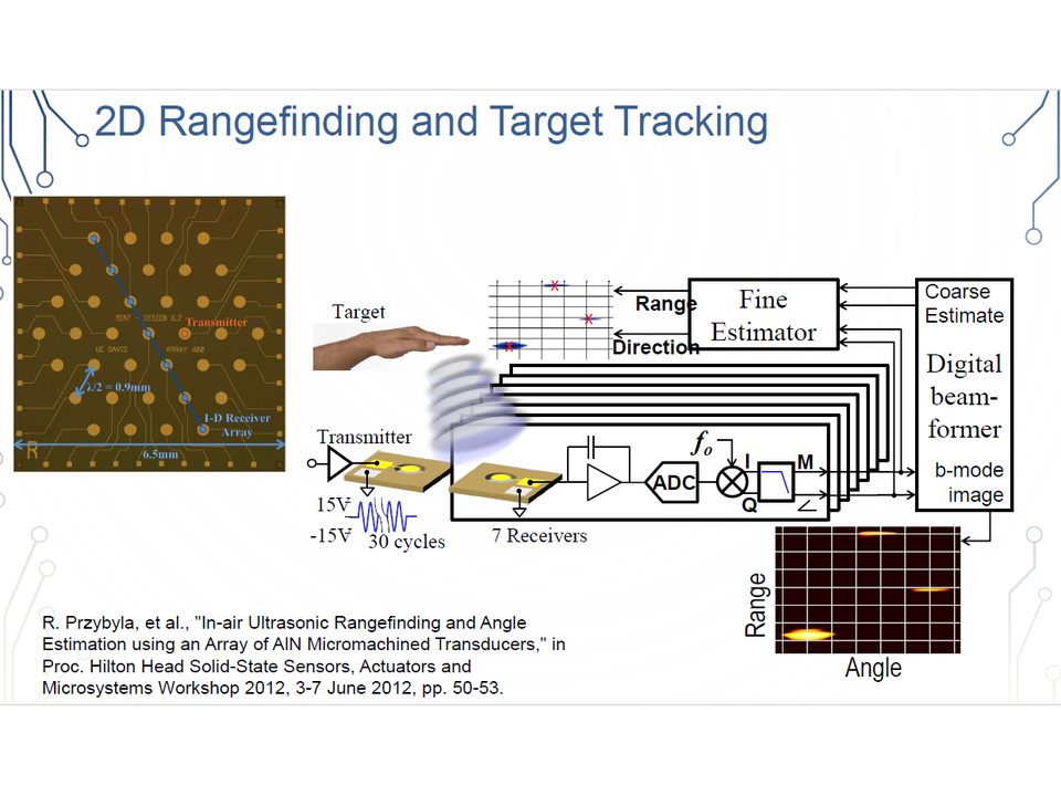
A figure from the published rangefinder paper: the transducer array, the readout chain, and a plot of range and angle tracking a target.

Ultrasonic rangefinder

MASS PRODUCTION

TDK-Chirp Microsystems · IoT

A time-of-flight rangefinder on a chip, small enough and low-power enough to sit in a consumer device. Precision frequency demodulation and low-jitter time measurement are what make a centimetre-scale echo readable at microwatt power.

Analog designer, prototype and first production generation · high-voltage pulser, PLL and frequency demodulation, mixer and filter design

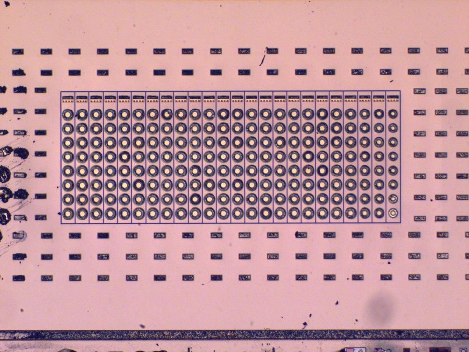
An optical micrograph of a rectangular transducer array, hundreds of circular elements laid out in a regular grid on a pink-toned substrate.

3-D ultrasonic fingerprint sensor-on-a-chip

RESEARCH

UC Berkeley · 2012-2016 · productized

The thesis chip. A PMUT array bonded to CMOS that images a fingerprint in three dimensions, including the ridge structure below the skin surface. It became the prototype for a commercial fingerprint sensor product line.

Chip lead and inventor · array and circuit co-design, high-voltage pulser, beamforming

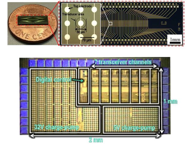
A published die photograph of the pulser chip, its transceiver channels and two charge pumps labelled, beside the packaged part on a coin.

High-efficiency piezo pulser with integrated charge pump

RESEARCH

UC Berkeley · 2013-2015 · medical and fitness

A handheld, battery-powered ultrasound imager demonstrated at ISSCC. The interesting part is the drive side: getting enough voltage into a discrete piezo element from a battery, efficiently enough that the whole instrument runs at milliwatts.

Chip lead · high-voltage drive, integrated charge pump

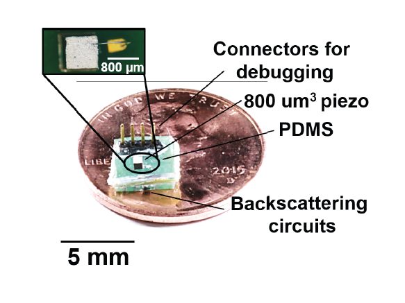
A published photograph of a millimetre-scale neural dust mote on a coin, with its piezo element and backscattering circuits labelled.

Neural Dust piezo implant ASIC

RESEARCH

UC Berkeley · 2013-2016 · neural interfaces

A millimetre-scale implant that records neural activity and is powered and read out by ultrasound through tissue, with no battery and no wire. I built the ASIC the prototype used; the work went on to seed iota Biosciences.

ASIC provider · ASIC design, ultrasound wireless power transfer

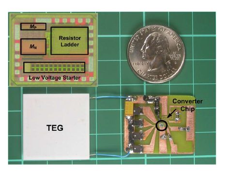
A published photograph of the energy-harvesting test board: the converter chip, a thermoelectric generator, and a coin for scale.

50 mV-input batteryless boost converter

RESEARCH

National Taiwan University · 2011-2013 · energy harvesting

A DC-DC converter that starts up from 50 mV with no battery and no external kick, turning the few tens of millivolts a thermoelectric generator produces into a usable supply rail. My first silicon, and still my second most-cited paper.

Chip lead · converter architecture, startup circuit

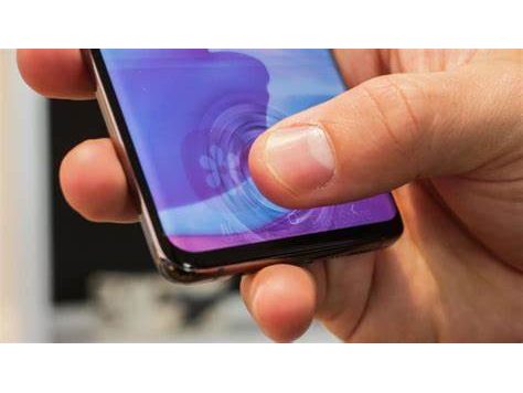
A hand holding a smartphone with a fingertip on the in-display ultrasonic fingerprint area.

3D Sonic fingerprint sensor

MASS PRODUCTION

Qualcomm · mobile

A large-area ultrasonic fingerprint sensor built on a thin-film transistor backplane with a piezoelectric polymer film, driven by a companion ASIC.

Analog designer · high-voltage drive, transmit beamforming

Publications